当前位置:
X-MOL 学术
›
ACS Appl. Mater. Interfaces
›
论文详情
Our official English website, www.x-mol.net, welcomes your feedback! (Note: you will need to create a separate account there.)
Growth of Wafer-Scale Standing Layers of WS2 for Self-Biased High-Speed UV–Visible–NIR Optoelectronic Devices
ACS Applied Materials & Interfaces ( IF 9.5 ) Pub Date : 2018-01-16 00:00:00 , DOI: 10.1021/acsami.7b16397 Hong-Sik Kim 1 , Malkeshkumar Patel , Joondong Kim , Mun Seok Jeong 1
ACS Applied Materials & Interfaces ( IF 9.5 ) Pub Date : 2018-01-16 00:00:00 , DOI: 10.1021/acsami.7b16397 Hong-Sik Kim 1 , Malkeshkumar Patel , Joondong Kim , Mun Seok Jeong 1
Affiliation
|
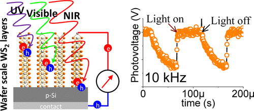
This work describes the wafer-scale standing growth of (002)-plane-oriented layers of WS2 and their suitability for use in self-biased broad-band high-speed photodetection. The WS2 layers are grown using large-scale sputtering, and the effects of the processing parameters such as the deposition temperature, deposition time, and sputtering power are studied. The structural, physical, chemical, optical, and electrical properties of the WS2 samples are also investigated. On the basis of the broad-band light absorption and high-speed in-plane carrier transport characteristics of the WS2 layers, a self-biased broad-band high-speed photodetector is fabricated by forming a type-II heterojunction. This WS2/Si heterojunction is sensitive to ultraviolet, visible, and near-infrared photons and shows an ultrafast photoresponse (1.1 μs) along with an excellent responsivity (4 mA/W) and a specific detectivity (∼1.5 × 10¹⁰ Jones). A comprehensive Mott–Schottky analysis is performed to evaluate the parameters of the device, such as the frequency-dependent flat-band potential and carrier concentration. Further, the photodetection parameters of the device, such as its linear dynamic range, rising time, and falling time, are evaluated to elucidate its spectral and transient characteristics. The device exhibits remarkably improved transient and spectral photodetection performances as compared to those of photodetectors based on atomically thin WS2 and two-dimensional materials. These results suggest that the proposed method is feasible for the manipulation of vertically standing WS2 layers that exhibit high in-plane carrier mobility and allow for high-performance broad-band photodetection and energy device applications.
中文翻译:

用于自偏置高速紫外可见可见近红外光电器件的WS 2晶圆级站立层的生长
这项工作描述了WS 2面向(002)平面的层的晶圆级固定生长及其在自偏置宽带高速光电检测中的适用性。使用大规模溅射法生长WS 2层,并研究诸如沉积温度,沉积时间和溅射功率等工艺参数的影响。还研究了WS 2样品的结构,物理,化学,光学和电学性质。根据WS 2层的宽带光吸收和高速面内载流子传输特性,通过形成II型异质结来制造自偏置宽带高速光电探测器。WS 2/ Si异质结对紫外线,可见光和近红外光子敏感,并显示出超快的光响应(1.1μs)以及出色的响应度(4 mA / W)和特定的检测率(〜1.5×10 10 Jones)。进行了全面的Mott–Schottky分析,以评估设备的参数,例如与频率有关的平带电势和载波浓度。此外,对器件的光电检测参数(例如其线性动态范围,上升时间和下降时间)进行评估,以阐明其光谱和瞬态特性。与基于原子薄WS 2的光电探测器相比,该器件具有显着改善的瞬态和光谱光电探测性能和二维材料。这些结果表明,所提出的方法对于处理垂直WS 2层是可行的,该WS 2层显示出高的面内载流子迁移率并允许高性能宽带光电检测和能量设备应用。
更新日期:2018-01-16
中文翻译:
用于自偏置高速紫外可见可见近红外光电器件的WS 2晶圆级站立层的生长
这项工作描述了WS 2面向(002)平面的层的晶圆级固定生长及其在自偏置宽带高速光电检测中的适用性。使用大规模溅射法生长WS 2层,并研究诸如沉积温度,沉积时间和溅射功率等工艺参数的影响。还研究了WS 2样品的结构,物理,化学,光学和电学性质。根据WS 2层的宽带光吸收和高速面内载流子传输特性,通过形成II型异质结来制造自偏置宽带高速光电探测器。WS 2/ Si异质结对紫外线,可见光和近红外光子敏感,并显示出超快的光响应(1.1μs)以及出色的响应度(4 mA / W)和特定的检测率(〜1.5×10 10 Jones)。进行了全面的Mott–Schottky分析,以评估设备的参数,例如与频率有关的平带电势和载波浓度。此外,对器件的光电检测参数(例如其线性动态范围,上升时间和下降时间)进行评估,以阐明其光谱和瞬态特性。与基于原子薄WS 2的光电探测器相比,该器件具有显着改善的瞬态和光谱光电探测性能和二维材料。这些结果表明,所提出的方法对于处理垂直WS 2层是可行的,该WS 2层显示出高的面内载流子迁移率并允许高性能宽带光电检测和能量设备应用。


 京公网安备 11010802027423号