当前位置:
X-MOL 学术
›
ACS Appl. Mater. Interfaces
›
论文详情
Our official English website, www.x-mol.net, welcomes your
feedback! (Note: you will need to create a separate account there.)
Probing the Dielectric Properties of Ultrathin Al/Al2O3/Al Trilayers Fabricated Using in Situ Sputtering and Atomic Layer Deposition
ACS Applied Materials & Interfaces ( IF 8.3 ) Pub Date : 2018-01-12 00:00:00 , DOI: 10.1021/acsami.7b16506 Jagaran Acharya 1 , Jamie Wilt 1 , Bo Liu 1 , Judy Wu 1
ACS Applied Materials & Interfaces ( IF 8.3 ) Pub Date : 2018-01-12 00:00:00 , DOI: 10.1021/acsami.7b16506 Jagaran Acharya 1 , Jamie Wilt 1 , Bo Liu 1 , Judy Wu 1
Affiliation
|
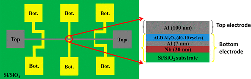
Dielectric properties of ultrathin Al2O3 (1.1–4.4 nm) in metal–insulator–metal (M–I–M) Al/Al2O3/Al trilayers fabricated in situ using an integrated sputtering and atomic layer deposition (ALD) system were investigated. An M–I interfacial layer (IL) formed during the pre-ALD sample transfer even under high vacuum has a profound effect on the dielectric properties of the Al2O3 with a significantly reduced dielectric constant (εr) of 0.5–3.3 as compared to the bulk εr ∼ 9.2. Moreover, the observed soft-type electric breakdown suggests defects in both the M–I interface and the Al2O3 film. By controlling the pre-ALD exposure to reduce the IL to a negligible level, a high εr up to 8.9 was obtained on the ALD Al2O3 films with thicknesses from 3.3 to 4.4 nm, corresponding to an effective oxide thickness (EOT) of ∼1.4–1.9 nm, respectively, which are comparable to the EOTs found in high-K dielectrics like HfO2 at 3–4 nm in thickness and further suggest that the ultrathin ALD Al2O3 produced in optimal conditions may provide a low-cost alternative gate dielectric for CMOS. While εr decreases at a smaller Al2O3 thickness, the hard-type dielectric breakdown at 32 MV/cm and in situ scanning tunneling spectroscopy revealed band gap ∼2.63 eV comparable to that of an epitaxial Al2O3 film. This suggests that the IL is unlikely a dominant reason for the reduced εr at the Al2O3 thickness of 1.1–2.2 nm but rather a consequence of the electron tunneling as confirmed in the transport measurement. This result demonstrates the critical importance in controlling the IL to achieving high-performance ultrathin dielectric in MIM structures.
中文翻译:

探索原位溅射和原子层沉积制备的超薄Al / Al 2 O 3 / Al三层薄膜的介电性能
金属-绝缘体-金属(M-I-M)Al / Al 2 O 3 / Al三层通过集成溅射和原子层沉积(ALD)原位制造的超薄Al 2 O 3(1.1-4.4 nm)的介电性能系统进行了调查。即使在高真空下,在ALD前样品转移过程中形成的M–I界面层(IL)也会对Al 2 O 3的介电性能产生深远的影响,介电常数(εr)会显着降低,为0.5–3.3。相比于块状ε - [R〜9.2。此外,观察到的软型电击穿表明M–I界面和Al 2 O均存在缺陷3片。通过控制ALD前暴露以将IL降低到可以忽略的水平,在厚度为3.3至4.4 nm的ALD Al 2 O 3膜上获得了高达8.9的高εr,相当于有效氧化物厚度(EOT)厚度分别约为1.4-1.9 nm,这与高K电介质(如HfO 2)在3-4 nm的厚度中发现的EOT相当,并且进一步表明,在最佳条件下生产的超薄ALD Al 2 O 3可能提供较低的成本的CMOS替代栅极电介质。而在较小的Al 2 O 3下εr减小厚度,在32 MV / cm处的硬型介电击穿和原位扫描隧穿光谱显示,带隙约为2.63 eV,与外延Al 2 O 3膜相当。这表明,IL不太可能是Al 2 O 3厚度为1.1–2.2 nm时εr降低的主要原因,而是传输测量中证实的电子隧穿的结果。该结果证明了在控制IL以实现MIM结构中的高性能超薄电介质方面至关重要。
更新日期:2018-01-12
中文翻译:
探索原位溅射和原子层沉积制备的超薄Al / Al 2 O 3 / Al三层薄膜的介电性能
金属-绝缘体-金属(M-I-M)Al / Al 2 O 3 / Al三层通过集成溅射和原子层沉积(ALD)原位制造的超薄Al 2 O 3(1.1-4.4 nm)的介电性能系统进行了调查。即使在高真空下,在ALD前样品转移过程中形成的M–I界面层(IL)也会对Al 2 O 3的介电性能产生深远的影响,介电常数(εr)会显着降低,为0.5–3.3。相比于块状ε - [R〜9.2。此外,观察到的软型电击穿表明M–I界面和Al 2 O均存在缺陷3片。通过控制ALD前暴露以将IL降低到可以忽略的水平,在厚度为3.3至4.4 nm的ALD Al 2 O 3膜上获得了高达8.9的高εr,相当于有效氧化物厚度(EOT)厚度分别约为1.4-1.9 nm,这与高K电介质(如HfO 2)在3-4 nm的厚度中发现的EOT相当,并且进一步表明,在最佳条件下生产的超薄ALD Al 2 O 3可能提供较低的成本的CMOS替代栅极电介质。而在较小的Al 2 O 3下εr减小厚度,在32 MV / cm处的硬型介电击穿和原位扫描隧穿光谱显示,带隙约为2.63 eV,与外延Al 2 O 3膜相当。这表明,IL不太可能是Al 2 O 3厚度为1.1–2.2 nm时εr降低的主要原因,而是传输测量中证实的电子隧穿的结果。该结果证明了在控制IL以实现MIM结构中的高性能超薄电介质方面至关重要。


 京公网安备 11010802027423号