当前位置:
X-MOL 学术
›
Adv. Electron. Mater.
›
论文详情
Our official English website, www.x-mol.net, welcomes your
feedback! (Note: you will need to create a separate account there.)
Transparent Nanoscale Polyimide Gate Dielectric for Highly Flexible Electronics
Advanced Electronic Materials ( IF 5.3 ) Pub Date : 2018-01-02 , DOI: 10.1002/aelm.201700043 Saungeun Park 1 , Hsiao-Yu Chang 1 , Somayyeh Rahimi 1 , Alvin L. Lee 1 , Li Tao 1 , Deji Akinwande 1
Advanced Electronic Materials ( IF 5.3 ) Pub Date : 2018-01-02 , DOI: 10.1002/aelm.201700043 Saungeun Park 1 , Hsiao-Yu Chang 1 , Somayyeh Rahimi 1 , Alvin L. Lee 1 , Li Tao 1 , Deji Akinwande 1
Affiliation
|
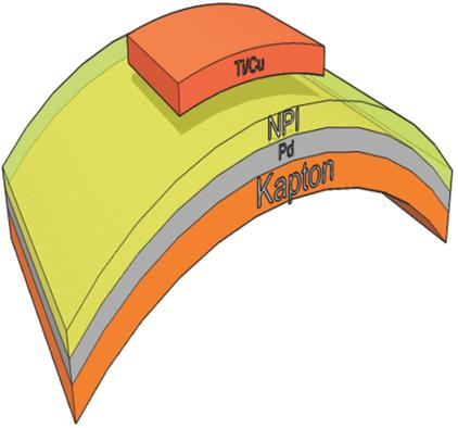
Transparent and solution‐processable nanoscale polyimide (NPI) films less than 100 nm thick and their applications as flexible gate dielectrics for 2D‐materials‐based transistor devices are reported. Stable electrical performances of NPI dielectric under high tensile strains up to 10% are demonstrated by in situ bending experiments. A welcome benefit of the NPI nanoscale thickness is that the optical transparency is improved over 84% across the visible spectrum compared to conventional thick polyimide, indicating suitability for transparent electronics, such as displays and sensors. Prototypical 2D active materials, molybdenum disulfide (MoS2), and graphene using NPI gate dielectric show outstanding thin‐film transistors (TFTs) properties comparable to performances of similar devices using atomic layer deposition (ALD) gate dielectrics. For instance, MoS2 FETs with NPI dielectric affords maximum field‐effect mobility of 30 cm2 V−1 s−1 and ON/OFF current ratio >107. Graphene FETs (GFETs), fabricated with NPI dielectric, also show DC and radio frequency (RF) performances comparable to similar devices with high‐κ dielectrics, such as maximum carrier mobility of ≈5170 cm2 V−1 s−1. An extrinsic cutoff frequency ≈6.5 GHz is achieved, which reveals that NPI is also a suitable dielectric for flexible RF TFTs for wireless communication systems.
中文翻译:

透明纳米级聚酰亚胺栅极电介质,用于高度柔性电子
报道了厚度小于100 nm的透明且可溶液处理的纳米级聚酰亚胺(NPI)膜及其在基于2D材料的晶体管器件中作为柔性栅极电介质的应用。通过原位弯曲实验证明了NPI电介质在高达10%的高拉伸应变下的稳定电性能。NPI纳米级厚度的一个令人欢迎的好处是,与常规的厚聚酰亚胺相比,在可见光谱范围内的光学透明性提高了84%以上,表明适用于诸如显示器和传感器之类的透明电子产品。典型的2D活性材料,二硫化钼(MoS 2)以及使用NPI栅极电介质的石墨烯具有出色的薄膜晶体管(TFT)性能,可与使用原子层沉积(ALD)栅极电介质的类似器件的性能相比。例如,具有NPI电介质的MoS 2 FET可提供30 cm 2 V -1 s -1的最大场效应迁移率,且开/关电流比> 10 7。用NPI电介质制造的石墨烯FET(GFET)也显示出与具有高κ电介质的类似器件相当的直流和射频(RF)性能,例如≈5170cm 2 V -1 s -1的最大载流子迁移率。外部截止频率约为6.5 GHz,这表明NPI还是适用于无线通信系统的柔性RF TFT的合适电介质。
更新日期:2018-01-02
中文翻译:
透明纳米级聚酰亚胺栅极电介质,用于高度柔性电子
报道了厚度小于100 nm的透明且可溶液处理的纳米级聚酰亚胺(NPI)膜及其在基于2D材料的晶体管器件中作为柔性栅极电介质的应用。通过原位弯曲实验证明了NPI电介质在高达10%的高拉伸应变下的稳定电性能。NPI纳米级厚度的一个令人欢迎的好处是,与常规的厚聚酰亚胺相比,在可见光谱范围内的光学透明性提高了84%以上,表明适用于诸如显示器和传感器之类的透明电子产品。典型的2D活性材料,二硫化钼(MoS 2)以及使用NPI栅极电介质的石墨烯具有出色的薄膜晶体管(TFT)性能,可与使用原子层沉积(ALD)栅极电介质的类似器件的性能相比。例如,具有NPI电介质的MoS 2 FET可提供30 cm 2 V -1 s -1的最大场效应迁移率,且开/关电流比> 10 7。用NPI电介质制造的石墨烯FET(GFET)也显示出与具有高κ电介质的类似器件相当的直流和射频(RF)性能,例如≈5170cm 2 V -1 s -1的最大载流子迁移率。外部截止频率约为6.5 GHz,这表明NPI还是适用于无线通信系统的柔性RF TFT的合适电介质。


 京公网安备 11010802027423号