Our official English website, www.x-mol.net, welcomes your feedback! (Note: you will need to create a separate account there.)
Toward Practical, Subwavelength, Visible-Light Photolithography with Hyperlens
ACS Nano ( IF 17.1 ) Pub Date : 2018-01-02 00:00:00 , DOI: 10.1021/acsnano.7b07185 Jingbo Sun 1 , Natalia M. Litchinitser 1
ACS Nano ( IF 17.1 ) Pub Date : 2018-01-02 00:00:00 , DOI: 10.1021/acsnano.7b07185 Jingbo Sun 1 , Natalia M. Litchinitser 1
Affiliation
|
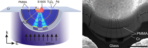
The future success of semiconductor technology relies on the continuing reduction of the feature size, allowing more components per chip and higher speed. Optical metamaterial-based hyperlens exhibit the ability for spatial pattern compression from the micro- to nanoscale, potentially addressing the ever-increasing demand of photolithograpy for inexpensive, all-optical nanoscale pattern recoding. Here, we demonstrate a photolithography system enabling a feature size of 80 nm using a 405 nm laser source. To realize such a system, we developed a fabrication method to obtain very thick hyperbolic metamaterial enabling a hyperlens with a very large demagnification rate of 3.75. Finally, we discuss several steps necessary to transform the proposed technique into a practical solution for the visible-light-based nanolithography. These include flattening of the inner surface of the hyperlens to increase the working area and integrating the proposed device into a conventional stepper system.
中文翻译:

利用超透镜实现实用的亚波长可见光光刻
半导体技术的未来成功取决于部件尺寸的不断减小,从而允许每个芯片更多的组件和更高的速度。基于光学超材料的超透镜展现了从微尺度到纳米尺度的空间图案压缩能力,潜在地满足了照相平版印刷对廉价,全光学的纳米尺度图案重新编码的不断增长的需求。在这里,我们演示了使用405 nm激光源实现80 nm特征尺寸的光刻系统。为了实现这样的系统,我们开发了一种制造方法来获得非常厚的双曲线超材料,从而使超透镜的放大倍率达到3.75。最后,我们讨论了将提议的技术转变为基于可见光的纳米光刻的实际解决方案所必需的几个步骤。
更新日期:2018-01-02
中文翻译:
利用超透镜实现实用的亚波长可见光光刻
半导体技术的未来成功取决于部件尺寸的不断减小,从而允许每个芯片更多的组件和更高的速度。基于光学超材料的超透镜展现了从微尺度到纳米尺度的空间图案压缩能力,潜在地满足了照相平版印刷对廉价,全光学的纳米尺度图案重新编码的不断增长的需求。在这里,我们演示了使用405 nm激光源实现80 nm特征尺寸的光刻系统。为了实现这样的系统,我们开发了一种制造方法来获得非常厚的双曲线超材料,从而使超透镜的放大倍率达到3.75。最后,我们讨论了将提议的技术转变为基于可见光的纳米光刻的实际解决方案所必需的几个步骤。


 京公网安备 11010802027423号