当前位置:
X-MOL 学术
›
Adv. Opt. Mater.
›
论文详情
Our official English website, www.x-mol.net, welcomes your
feedback! (Note: you will need to create a separate account there.)
Thermo‐optical Tunable Ultracompact Chip‐Integrated 1D Photonic Topological Insulator
Advanced Optical Materials ( IF 8.0 ) Pub Date : 2017-12-28 , DOI: 10.1002/adom.201701071 Chong Li 1 , Xiaoyong Hu 1, 2 , Wei Gao 1 , Yutian Ao 1 , Saisai Chu 1, 2 , Hong Yang 1, 2 , Qihuang Gong 1, 2
Advanced Optical Materials ( IF 8.0 ) Pub Date : 2017-12-28 , DOI: 10.1002/adom.201701071 Chong Li 1 , Xiaoyong Hu 1, 2 , Wei Gao 1 , Yutian Ao 1 , Saisai Chu 1, 2 , Hong Yang 1, 2 , Qihuang Gong 1, 2
Affiliation
|
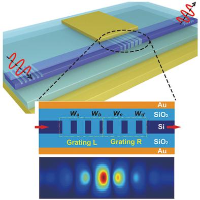
An on‐chip integrated one‐dimension topological insulator in the optical communication range is realized directly in an integrated photonic circuit. The system takes on a configuration of a 220 nm thick 1D photonic crystal heterostructure sandwiched between two gold films. A photonic topological edge state centered at 1550 nm is obtained for the chip‐integrated one‐dimension topological insulator made of a silicon/SiO2 photonic crystal heterostructure with a feature size of only 2.25 µm integrated with a silicon waveguide. On/off switching of the photonic topological edge state was also achieved in a 1D topological insulator made of a VO2/SiO2 photonic crystal heterostructure based on a thermally induced insulator‐to‐metal transition of VO2. This system not only paves the way for practical applications of photonic topological insulators in integrated photonic devices and chips but also provides a platform for fundamental studies of topological photonics.
中文翻译:

热光可调超紧凑芯片集成式一维光子拓扑绝缘子
直接在集成光子电路中实现光通信范围内的片上集成一维拓扑绝缘体。该系统采用夹在两个金膜之间的220 nm厚的一维光子晶体异质结构。对于由硅/ SiO 2光子晶体异质结构制成的芯片集成一维拓扑绝缘体,其特征尺寸仅为2.25 µm,并与硅波导集成在一起,可获得以1550 nm为中心的光子拓扑边缘状态。在由VO 2 / SiO 2光子晶体异质结构制成的一维拓扑绝缘体中,还基于热诱导的VO 2绝缘体-金属跃迁,实现了光子拓扑边缘状态的开/关切换。。该系统不仅为光子拓扑绝缘子在集成光子器件和芯片中的实际应用铺平了道路,而且为拓扑光子学的基础研究提供了平台。
更新日期:2017-12-28
中文翻译:
热光可调超紧凑芯片集成式一维光子拓扑绝缘子
直接在集成光子电路中实现光通信范围内的片上集成一维拓扑绝缘体。该系统采用夹在两个金膜之间的220 nm厚的一维光子晶体异质结构。对于由硅/ SiO 2光子晶体异质结构制成的芯片集成一维拓扑绝缘体,其特征尺寸仅为2.25 µm,并与硅波导集成在一起,可获得以1550 nm为中心的光子拓扑边缘状态。在由VO 2 / SiO 2光子晶体异质结构制成的一维拓扑绝缘体中,还基于热诱导的VO 2绝缘体-金属跃迁,实现了光子拓扑边缘状态的开/关切换。。该系统不仅为光子拓扑绝缘子在集成光子器件和芯片中的实际应用铺平了道路,而且为拓扑光子学的基础研究提供了平台。


 京公网安备 11010802027423号