当前位置:
X-MOL 学术
›
Adv. Electron. Mater.
›
论文详情
Our official English website, www.x-mol.net, welcomes your
feedback! (Note: you will need to create a separate account there.)
The Impact of Molecular p‐Doping on Charge Transport in High‐Mobility Small‐Molecule/Polymer Blend Organic Transistors
Advanced Electronic Materials ( IF 5.3 ) Pub Date : 2017-12-27 , DOI: 10.1002/aelm.201700464 Alexandra F. Paterson 1 , Yen-Hung Lin 2 , Alexander D. Mottram 3 , Zhuping Fei 4 , Muhammad R. Niazi 1 , Ahmad R. Kirmani 1 , Aram Amassian 1 , Olga Solomeshch 5 , Nir Tessler 5 , Martin Heeney 4 , Thomas D. Anthopoulos 1
Advanced Electronic Materials ( IF 5.3 ) Pub Date : 2017-12-27 , DOI: 10.1002/aelm.201700464 Alexandra F. Paterson 1 , Yen-Hung Lin 2 , Alexander D. Mottram 3 , Zhuping Fei 4 , Muhammad R. Niazi 1 , Ahmad R. Kirmani 1 , Aram Amassian 1 , Olga Solomeshch 5 , Nir Tessler 5 , Martin Heeney 4 , Thomas D. Anthopoulos 1
Affiliation
|
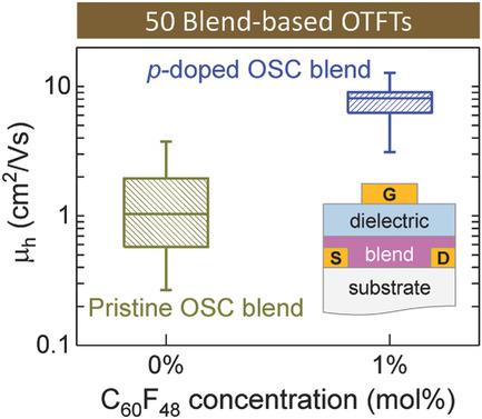
Molecular doping is a powerful tool with the potential to resolve many of the issues currently preventing organic thin‐film transistor (OTFT) commercialization. However, the addition of dopant molecules into organic semiconductors often disrupts the host lattice, introducing defects and harming electrical transport. New dopant‐based systems that overcome practical utilization issues, while still reaping the electrical performance benefits, would therefore be extremely valuable. Here, the impact of p‐doping on the charge transport in blends consisting of the small‐molecule 2,7‐dioctyl[1]benzothieno[3,2‐b][1]benzothiophene (C8‐BTBT), the polymer indacenodithiophene‐benzothiadiazole (C16IDT‐BT), and the molecular dopant C60F48 is investigated. Electrical field‐effect measurements indicate that p‐doping not only enhances the average saturation mobility from 1.4 to 7.8 cm2 V−1 s−1 over 50 devices (maximum values from around 4 to 13 cm2 V−1 s−1), but also improves bias–stress stability, contact resistance, threshold voltage, and the overall device‐to‐device performance variation. Importantly, materials characterization using X‐ray diffraction, X‐ray photoemission spectroscopy, and ultraviolet photoemission spectroscopy, combined with charge transport modeling, reveal that effective doping is achieved without perturbing the microstructure of the polycrystalline semiconductor film. This work highlights the remarkable potential of ternary organic blends as a simple platform for OTFTs to achieve all the benefits of doping, with none of the drawbacks.
中文翻译:

分子p掺杂对高迁移率小分子/聚合物共混有机晶体管中电荷传输的影响
分子掺杂是一种强大的工具,具有解决当前阻止有机薄膜晶体管(OTFT)商业化的许多问题的潜力。但是,将掺杂剂分子添加到有机半导体中通常会破坏主体晶格,从而引入缺陷并损害电传输。因此,新型的基于掺杂剂的系统在克服了实际使用问题的同时仍能获得电气性能上的好处,因此将具有极大的价值。在这里,p掺杂对由小分子2,7-二辛基[1]苯并噻吩并[3,2- b ] [1]苯并噻吩(C8-BTBT),聚合物茚并二噻吩-组成的共混物中电荷传输的影响苯并噻二唑(C16IDT-BT)和分子掺杂剂C 60 F 48被调查。电场效应测量表明,p掺杂不仅可以将50个器件的平均饱和迁移率从1.4提升至7.8 cm 2 V -1 s -1(最大值从4到13 cm 2 V -1 s -1左右)),还可以改善偏置应力的稳定性,接触电阻,阈值电压以及整个器件之间的性能差异。重要的是,使用X射线衍射,X射线光电子能谱和紫外光电子能谱对材料进行表征,再结合电荷传输模型,可以实现有效的掺杂而不会干扰多晶半导体膜的微观结构。这项工作强调了三元有机共混物作为OTFT的简单平台所具有的巨大潜力,可以实现掺杂的所有好处,而没有任何缺点。
更新日期:2017-12-27
中文翻译:
分子p掺杂对高迁移率小分子/聚合物共混有机晶体管中电荷传输的影响
分子掺杂是一种强大的工具,具有解决当前阻止有机薄膜晶体管(OTFT)商业化的许多问题的潜力。但是,将掺杂剂分子添加到有机半导体中通常会破坏主体晶格,从而引入缺陷并损害电传输。因此,新型的基于掺杂剂的系统在克服了实际使用问题的同时仍能获得电气性能上的好处,因此将具有极大的价值。在这里,p掺杂对由小分子2,7-二辛基[1]苯并噻吩并[3,2- b ] [1]苯并噻吩(C8-BTBT),聚合物茚并二噻吩-组成的共混物中电荷传输的影响苯并噻二唑(C16IDT-BT)和分子掺杂剂C 60 F 48被调查。电场效应测量表明,p掺杂不仅可以将50个器件的平均饱和迁移率从1.4提升至7.8 cm 2 V -1 s -1(最大值从4到13 cm 2 V -1 s -1左右)),还可以改善偏置应力的稳定性,接触电阻,阈值电压以及整个器件之间的性能差异。重要的是,使用X射线衍射,X射线光电子能谱和紫外光电子能谱对材料进行表征,再结合电荷传输模型,可以实现有效的掺杂而不会干扰多晶半导体膜的微观结构。这项工作强调了三元有机共混物作为OTFT的简单平台所具有的巨大潜力,可以实现掺杂的所有好处,而没有任何缺点。


 京公网安备 11010802027423号