当前位置:
X-MOL 学术
›
Adv. Mater. Interfaces
›
论文详情
Our official English website, www.x-mol.net, welcomes your
feedback! (Note: you will need to create a separate account there.)
In Situ Electrical Properties’ Investigation and Nanofabrication of Ag/Sb2Te3 Assembled Multilayers’ Film
Advanced Materials Interfaces ( IF 4.3 ) Pub Date : 2017-12-22 , DOI: 10.1002/admi.201701210 Zhenhua Wu 1 , Xiang Chen 2 , Yan Zhang 3 , Chaochao Dun 4 , David L. Carroll 4 , Zhiyu Hu 5
Advanced Materials Interfaces ( IF 4.3 ) Pub Date : 2017-12-22 , DOI: 10.1002/admi.201701210 Zhenhua Wu 1 , Xiang Chen 2 , Yan Zhang 3 , Chaochao Dun 4 , David L. Carroll 4 , Zhiyu Hu 5
Affiliation
|
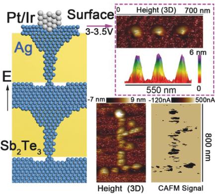
Nanopatterned fabrication and electrical properties of Ag/Sb2Te3 layer‐by‐layer assembled films are systematically investigated by a conductive atomic force microscope. Multilayers’ film composed by alternating Ag and Sb2Te3 with respective thicknesses of 5 and 10 nm shows a bipolar resistive switching behavior contributed by the silver conductive filaments. Designed cross‐plane nanofilament arrays with reconfigurable patterns are fabricated, which show a potential application in memristor and nanofabrication. Multilayers with the same thickness of Ag but increased thickness of Sb2Te3 (up to 20 nm) present a Fowler–Nordheim tunneling‐dominated current and show in‐plane snowflake silver dendrite on the surface. Further studies on the silver dendrite may bring potential applications in extensive fields such as multifunctional data storage and neuromorphic. By controlling the type (Sb2Te3, Bi2Te3, etc.) and thickness of solid electrolyte materials, electronic devices with specific functions and applications can be designed.
中文翻译:

Ag / Sb2Te3多层膜的原位电学研究及其纳米加工
用导电原子力显微镜系统地研究了Ag / Sb 2 Te 3逐层组装膜的纳米图案化制备和电学性能。由厚度分别为5和10 nm的Ag和Sb 2 Te 3交替组成的多层膜显示出由银导电丝引起的双极电阻切换行为。制备了具有可重构图案的设计的跨平面纳米丝阵列,显示出在忆阻器和纳米加工中的潜在应用。Ag厚度相同但Sb 2 Te 3厚度增加的多层(最大20 nm)呈现Fowler–Nordheim隧穿为主的电流,并在表面显示平面内雪花银枝晶。对银枝晶的进一步研究可能会在诸如多功能数据存储和神经形态学等广泛领域中带来潜在的应用。通过控制固体电解质材料的类型(Sb 2 Te 3,Bi 2 Te 3等)和厚度,可以设计具有特定功能和应用的电子设备。
更新日期:2017-12-22
中文翻译:
Ag / Sb2Te3多层膜的原位电学研究及其纳米加工
用导电原子力显微镜系统地研究了Ag / Sb 2 Te 3逐层组装膜的纳米图案化制备和电学性能。由厚度分别为5和10 nm的Ag和Sb 2 Te 3交替组成的多层膜显示出由银导电丝引起的双极电阻切换行为。制备了具有可重构图案的设计的跨平面纳米丝阵列,显示出在忆阻器和纳米加工中的潜在应用。Ag厚度相同但Sb 2 Te 3厚度增加的多层(最大20 nm)呈现Fowler–Nordheim隧穿为主的电流,并在表面显示平面内雪花银枝晶。对银枝晶的进一步研究可能会在诸如多功能数据存储和神经形态学等广泛领域中带来潜在的应用。通过控制固体电解质材料的类型(Sb 2 Te 3,Bi 2 Te 3等)和厚度,可以设计具有特定功能和应用的电子设备。


 京公网安备 11010802027423号