当前位置:
X-MOL 学术
›
CrystEngComm
›
论文详情
Our official English website, www.x-mol.net, welcomes your
feedback! (Note: you will need to create a separate account there.)
Design and epitaxial growth of quality-enhanced crack-free GaN films on AlN/Al heterostructures and their nucleation mechanism
CrystEngComm ( IF 2.6 ) Pub Date : 2017-12-20 00:00:00 , DOI: 10.1039/c7ce01995e Wenliang Wang 1, 2, 3, 4, 5 , Yulin Zheng 1, 2, 3, 4 , Xiuye Zhang 1, 2, 3, 4 , Yuan Li 1, 2, 3, 4 , Zhenya Lu 2, 3, 4, 6, 7 , Guoqiang Li 1, 2, 3, 4, 5
CrystEngComm ( IF 2.6 ) Pub Date : 2017-12-20 00:00:00 , DOI: 10.1039/c7ce01995e Wenliang Wang 1, 2, 3, 4, 5 , Yulin Zheng 1, 2, 3, 4 , Xiuye Zhang 1, 2, 3, 4 , Yuan Li 1, 2, 3, 4 , Zhenya Lu 2, 3, 4, 6, 7 , Guoqiang Li 1, 2, 3, 4, 5
Affiliation
|
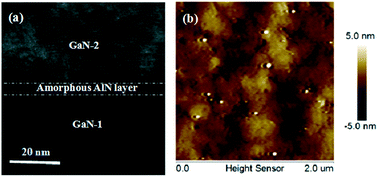
The epitaxial structures of GaN films grown on AlN/Al heterostructures by pulsed laser deposition (PLD) are designed with and without an amorphous AlN layer, and quality-enhanced crack-free GaN epitaxial films are obtained. Compared with GaN epitaxial films grown without inserting the amorphous AlN layer, by inserting a ∼5 nm-thick amorphous AlN layer in GaN, the residual stress in ∼600 nm-thick GaN epitaxial films is greatly reduced from −0.81 to −0.19 GPa, and high-density dislocations are annihilated in the amorphous AlN layer. The full-width at half-maximum for GaN(0002) and GaN(10-12) decreases from 1.1° and 1.2° to 0.90° and 0.98°, respectively. The root-mean-square surface roughness of as-grown GaN epitaxial films is also decreased from 3.5 to 1.5 nm. Evidently, the amorphous AlN layer can release the stress and trap the dislocations, preventing them from extending into the upper layer, as well as improve the surface morphology of GaN epitaxial films. Moreover, the nucleation mechanism of dislocation formation and annihilation in GaN epitaxial films grown on AlN/Al heterostructures by PLD with an amorphous AlN layer is hence proposed. These quality-enhanced GaN epitaxial films are of paramount importance for the application of GaN-based optoelectronic devices.
中文翻译:

AlN / Al异质结构上优质无裂纹GaN薄膜的设计,外延生长及其成核机理
设计了在有或没有非晶态AlN层的情况下,通过脉冲激光沉积(PLD)在AlN / Al异质结构上生长的GaN膜的外延结构,从而获得了质量提高的无裂纹GaN外延膜。与不插入非晶AlN层而生长的GaN外延膜相比,通过在GaN中插入约5nm厚的非晶AlN层,将约600nm厚的GaN外延膜中的残余应力从-0.81降低至-0.19 GPa,在非晶AlN层中消除了高密度位错。GaN(0002)和GaN(10-12)的半峰全宽分别从1.1°和1.2°降至0.90°和0.98°。所生长的GaN外延膜的均方根表面粗糙度也从3.5nm降低至1.5nm。显然,非晶AlN层可以释放应力并捕获位错,防止它们延伸到上层,并改善GaN外延膜的表面形态。此外,因此提出了通过具有非晶AlN层的PLD在AlN / Al异质结构上生长的GaN外延膜中的位错形成和an没的成核机理。这些质量增强的GaN外延膜对于基于GaN的光电器件的应用至关重要。
更新日期:2017-12-20
中文翻译:
AlN / Al异质结构上优质无裂纹GaN薄膜的设计,外延生长及其成核机理
设计了在有或没有非晶态AlN层的情况下,通过脉冲激光沉积(PLD)在AlN / Al异质结构上生长的GaN膜的外延结构,从而获得了质量提高的无裂纹GaN外延膜。与不插入非晶AlN层而生长的GaN外延膜相比,通过在GaN中插入约5nm厚的非晶AlN层,将约600nm厚的GaN外延膜中的残余应力从-0.81降低至-0.19 GPa,在非晶AlN层中消除了高密度位错。GaN(0002)和GaN(10-12)的半峰全宽分别从1.1°和1.2°降至0.90°和0.98°。所生长的GaN外延膜的均方根表面粗糙度也从3.5nm降低至1.5nm。显然,非晶AlN层可以释放应力并捕获位错,防止它们延伸到上层,并改善GaN外延膜的表面形态。此外,因此提出了通过具有非晶AlN层的PLD在AlN / Al异质结构上生长的GaN外延膜中的位错形成和an没的成核机理。这些质量增强的GaN外延膜对于基于GaN的光电器件的应用至关重要。


 京公网安备 11010802027423号