当前位置:
X-MOL 学术
›
Acc. Chem. Res.
›
论文详情
Our official English website, www.x-mol.net, welcomes your feedback! (Note: you will need to create a separate account there.)
Structure/Property Relations in “Giant” Semiconductor Nanocrystals: Opportunities in Photonics and Electronics
Accounts of Chemical Research ( IF 18.3 ) Pub Date : 2017-12-20 00:00:00 , DOI: 10.1021/acs.accounts.7b00467 Fabiola Navarro-Pardo 1, 2 , Haiguang Zhao 3 , Zhiming M. Wang 1 , Federico Rosei 1, 2
Accounts of Chemical Research ( IF 18.3 ) Pub Date : 2017-12-20 00:00:00 , DOI: 10.1021/acs.accounts.7b00467 Fabiola Navarro-Pardo 1, 2 , Haiguang Zhao 3 , Zhiming M. Wang 1 , Federico Rosei 1, 2
Affiliation
|
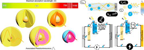
Semiconductor nanocrystals exhibit size-tunable absorption and emission ranging from the ultraviolet (UV) to the near-infrared (NIR) spectral range, high absorption coefficient, and high photoluminescence quantum yield. Effective surface passivation of these so-called quantum dots (QDs) may be achieved by growing a shell of another semiconductor material. The resulting core/shell QDs can be considered as a model system to study and optimize structure/property relations. A special case consists in growing thick shells (1.5 up to few tens of nanometers) to produce “giant” QDs (g-QDs). Tailoring the chemical composition and structure of CdSe/CdS and PbS/CdS g-QDs is a promising approach to widen the spectral separation of absorption and emission spectra (i.e., the Stokes shift), improve the isolation of photogenerated carriers from surface defects and enhance charge carrier lifetime and mobility. However, most stable systems are limited by a thick CdS shell, which strongly absorbs radiation below 500 nm, covering the UV and part of the visible range. Modification of the interfacial region between the core and shell of g-QDs or tuning their doping with narrow band gap semiconductors are effective approaches to circumvent this challenge. In addition, the synthesis of g-QDs composed of environmentally friendly elements (e.g., CuInSe2/CuInS2) represents an alternative to extend their absorption into the NIR range. Additionally, the band gap and band alignment of g-QDs can be engineered by proper selection of the constituents according to their band edge positions and by tuning their stoichiometry during wet chemical synthesis. In most cases, the quasi-type II localization regime of electrons and holes is achieved. In this type of g-QDs, electrons can leak into the shell region, while the holes remain confined within the core region. This electron–hole spatial distribution is advantageous for optoelectronic devices, resulting in efficient electron–hole separation while maintaining good stability.
中文翻译:

“巨型”半导体纳米晶体中的结构/性质关系:光子学和电子学中的机会
半导体纳米晶体的尺寸可调吸收和发射范围从紫外线(UV)到近红外(NIR)光谱范围,高吸收系数和高光致发光量子产率。这些所谓的量子点(QD)的有效表面钝化可以通过生长另一种半导体材料的壳来实现。产生的核/壳QD可以视为研究和优化结构/性质关系的模型系统。一种特殊情况是生长厚壳(1.5到几十纳米)以生产“巨型”量子点(g-QD)。量身定制CdSe / CdS和PbS / CdS g-QDs的化学成分和结构是扩大吸收光谱和发射光谱的光谱分离(即斯托克斯位移)的一种有前途的方法,改善了光生载流子与表面缺陷的隔离,并延长了载流子寿命和迁移率。但是,大多数稳定的系统都受到厚厚的CdS外壳的限制,该外壳会强烈吸收500 nm以下的辐射,覆盖UV和可见范围的一部分。修改g-QD核与壳之间的界面区域或使用窄带隙半导体调节其掺杂是解决这一挑战的有效方法。此外,由环境友好元素(例如CuInSe)组成的g-QD的合成 修改g-QD核与壳之间的界面区域或使用窄带隙半导体调节其掺杂是解决这一挑战的有效方法。此外,由环境友好元素(例如CuInSe)组成的g-QD的合成 修改g-QD核与壳之间的界面区域或使用窄带隙半导体调节其掺杂是解决这一挑战的有效方法。此外,由环境友好元素(例如CuInSe)组成的g-QD的合成2 / CuInS 2)表示将其吸收范围扩展到NIR范围的替代方法。此外,G-量子点的带隙和带对准可以通过各组分的适当选择,根据其能带边缘位置和通过在湿化学合成调谐它们的化学计量设计的。在大多数情况下,可以实现电子和空穴的准II型定位机制。在这种类型的g-QD中,电子可以泄漏到壳区中,而空穴仍被限制在核区中。这种电子-空穴的空间分布对于光电器件是有利的,从而在保持良好稳定性的同时实现了有效的电子-空穴分离。
更新日期:2017-12-20
中文翻译:
“巨型”半导体纳米晶体中的结构/性质关系:光子学和电子学中的机会
半导体纳米晶体的尺寸可调吸收和发射范围从紫外线(UV)到近红外(NIR)光谱范围,高吸收系数和高光致发光量子产率。这些所谓的量子点(QD)的有效表面钝化可以通过生长另一种半导体材料的壳来实现。产生的核/壳QD可以视为研究和优化结构/性质关系的模型系统。一种特殊情况是生长厚壳(1.5到几十纳米)以生产“巨型”量子点(g-QD)。量身定制CdSe / CdS和PbS / CdS g-QDs的化学成分和结构是扩大吸收光谱和发射光谱的光谱分离(即斯托克斯位移)的一种有前途的方法,改善了光生载流子与表面缺陷的隔离,并延长了载流子寿命和迁移率。但是,大多数稳定的系统都受到厚厚的CdS外壳的限制,该外壳会强烈吸收500 nm以下的辐射,覆盖UV和可见范围的一部分。修改g-QD核与壳之间的界面区域或使用窄带隙半导体调节其掺杂是解决这一挑战的有效方法。此外,由环境友好元素(例如CuInSe)组成的g-QD的合成 修改g-QD核与壳之间的界面区域或使用窄带隙半导体调节其掺杂是解决这一挑战的有效方法。此外,由环境友好元素(例如CuInSe)组成的g-QD的合成 修改g-QD核与壳之间的界面区域或使用窄带隙半导体调节其掺杂是解决这一挑战的有效方法。此外,由环境友好元素(例如CuInSe)组成的g-QD的合成2 / CuInS 2)表示将其吸收范围扩展到NIR范围的替代方法。此外,G-量子点的带隙和带对准可以通过各组分的适当选择,根据其能带边缘位置和通过在湿化学合成调谐它们的化学计量设计的。在大多数情况下,可以实现电子和空穴的准II型定位机制。在这种类型的g-QD中,电子可以泄漏到壳区中,而空穴仍被限制在核区中。这种电子-空穴的空间分布对于光电器件是有利的,从而在保持良好稳定性的同时实现了有效的电子-空穴分离。


 京公网安备 11010802027423号