当前位置:
X-MOL 学术
›
Electroanalysis
›
论文详情
Our official English website, www.x-mol.net, welcomes your
feedback! (Note: you will need to create a separate account there.)
Direct Toner Printing: A Versatile Technology for Easy Fabrication of Flexible Miniaturized Electrodes
Electroanalysis ( IF 2.7 ) Pub Date : 2017-12-19 , DOI: 10.1002/elan.201700717 Everson T. S. G. da Silva 1, 2 , Thais M. R. Alves 1, 2 , Lauro T. Kubota 1, 2
Electroanalysis ( IF 2.7 ) Pub Date : 2017-12-19 , DOI: 10.1002/elan.201700717 Everson T. S. G. da Silva 1, 2 , Thais M. R. Alves 1, 2 , Lauro T. Kubota 1, 2
Affiliation
|
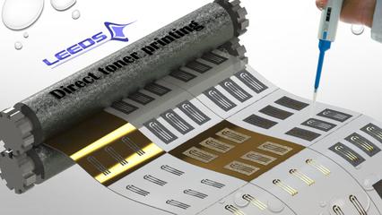
We reported here three simple, low cost and easy to accomplish strategies for the fabrication of microelectrodes and other conductive patterns using ordinary office laser‐printers. In this work, toner patterns were directly printed onto the flexible substrate, acting as a mask to create the intended conductive design. To highlight the versatility of such technology, toner‐printed patterns were employed in two diverse ways: one in which the patterned toner had the exact design of the electrode and other employing a reverse toner‐printed pattern. The first one was used for the adaptation of the well‐known printed circuit board (PCB) fabrication technique, but using direct toner printing (DTP) in an already conductive flexible substrate. The second was employed for the two remaining strategies: one based on the deposition of conductive film, followed by lift‐off process; and another based on drop‐casting of a conductive ink into the formed toner cavities, followed by thermal cure. As proof‐of‐concept, all three DTP strategies were used for the fabrication of miniaturized gold electrodes in polyimide substrate, and electrochemical performance of each obtained electrode was evaluated by cyclic voltammetry. Insights about DTP technology, alignment issues, advantages, limitations and resolution of each presented approach were provided. Finally, direct toner printing showed to be a simple, affordable and quite promising technology for the fabrication of low cost point‐of‐care electrochemical devices using flexible platforms.
中文翻译:

直接碳粉印刷:一种多功能的技术,可轻松制造柔性微型电极
我们在这里报告了三种使用普通办公室激光打印机制造微电极和其他导电图案的简单,低成本和易于完成的策略。在这项工作中,将墨粉图案直接印刷在柔性基板上,充当掩模以创建所需的导电设计。为了突出这种技术的多功能性,以两种不同的方式采用了碳粉打印的图案:一种是图案化的碳粉具有电极的精确设计,另一种采用了反向的碳粉打印图案。第一个用于改编众所周知的印刷电路板(PCB)制造技术,但在已经导电的柔性基板中使用直接碳粉印刷(DTP)。第二种用于剩余的两种策略:一种基于导电膜的沉积,随后进行提货过程; 另一个基于将导电油墨滴铸到形成的墨粉腔中,然后进行热固化。作为概念验证,所有三种DTP策略均用于在聚酰亚胺衬底中制备小型金电极,并通过循环伏安法评估每个获得的电极的电化学性能。提供了有关DTP技术,对齐问题,优点,局限性和每种提出的方法的解决方案的见解。最后,直接碳粉打印被证明是一种使用柔性平台制造低成本即时护理电化学设备的简单,可负担且非常有前途的技术。所有这三种DTP策略均用于在聚酰亚胺衬底中制备小型金电极,并通过循环伏安法评估每个获得的电极的电化学性能。提供了有关DTP技术,对齐问题,优点,局限性和每种提出的方法的解决方案的见解。最后,直接碳粉打印被证明是一种使用柔性平台制造低成本即时护理电化学设备的简单,可负担且非常有前途的技术。所有这三种DTP策略均用于在聚酰亚胺衬底中制备小型金电极,并通过循环伏安法评估每个获得的电极的电化学性能。提供了有关DTP技术,对齐问题,优点,局限性和每种提出的方法的解决方案的见解。最后,直接碳粉打印被证明是一种使用柔性平台制造低成本即时护理电化学设备的简单,可负担且非常有前途的技术。
更新日期:2017-12-19
中文翻译:
直接碳粉印刷:一种多功能的技术,可轻松制造柔性微型电极
我们在这里报告了三种使用普通办公室激光打印机制造微电极和其他导电图案的简单,低成本和易于完成的策略。在这项工作中,将墨粉图案直接印刷在柔性基板上,充当掩模以创建所需的导电设计。为了突出这种技术的多功能性,以两种不同的方式采用了碳粉打印的图案:一种是图案化的碳粉具有电极的精确设计,另一种采用了反向的碳粉打印图案。第一个用于改编众所周知的印刷电路板(PCB)制造技术,但在已经导电的柔性基板中使用直接碳粉印刷(DTP)。第二种用于剩余的两种策略:一种基于导电膜的沉积,随后进行提货过程; 另一个基于将导电油墨滴铸到形成的墨粉腔中,然后进行热固化。作为概念验证,所有三种DTP策略均用于在聚酰亚胺衬底中制备小型金电极,并通过循环伏安法评估每个获得的电极的电化学性能。提供了有关DTP技术,对齐问题,优点,局限性和每种提出的方法的解决方案的见解。最后,直接碳粉打印被证明是一种使用柔性平台制造低成本即时护理电化学设备的简单,可负担且非常有前途的技术。所有这三种DTP策略均用于在聚酰亚胺衬底中制备小型金电极,并通过循环伏安法评估每个获得的电极的电化学性能。提供了有关DTP技术,对齐问题,优点,局限性和每种提出的方法的解决方案的见解。最后,直接碳粉打印被证明是一种使用柔性平台制造低成本即时护理电化学设备的简单,可负担且非常有前途的技术。所有这三种DTP策略均用于在聚酰亚胺衬底中制备小型金电极,并通过循环伏安法评估每个获得的电极的电化学性能。提供了有关DTP技术,对齐问题,优点,局限性和每种提出的方法的解决方案的见解。最后,直接碳粉打印被证明是一种使用柔性平台制造低成本即时护理电化学设备的简单,可负担且非常有前途的技术。


 京公网安备 11010802027423号