Our official English website, www.x-mol.net, welcomes your
feedback! (Note: you will need to create a separate account there.)
Impact of Plasma Electron Flux on Plasma Damage‐Free Sputtering of Ultrathin Tin‐Doped Indium Oxide Contact Layer on p‐GaN for InGaN/GaN Light‐Emitting Diodes
Advanced Science ( IF 14.3 ) Pub Date : 2017-12-19 , DOI: 10.1002/advs.201700637 Kwang Jeong Son 1 , Tae Kyoung Kim 1 , Yu-Jung Cha 1 , Seung Kyu Oh 1, 2 , Shin-Jae You 3 , Jae-Hyun Ryou 2, 4 , Joon Seop Kwak 1
Advanced Science ( IF 14.3 ) Pub Date : 2017-12-19 , DOI: 10.1002/advs.201700637 Kwang Jeong Son 1 , Tae Kyoung Kim 1 , Yu-Jung Cha 1 , Seung Kyu Oh 1, 2 , Shin-Jae You 3 , Jae-Hyun Ryou 2, 4 , Joon Seop Kwak 1
Affiliation
|
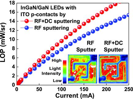
The origin of plasma‐induced damage on a p
‐type wide‐bandgap layer during the sputtering of tin‐doped indium oxide (ITO) contact layers by using radiofrequency‐superimposed direct current (DC) sputtering and its effects on the forward voltage and light output power (LOP) of light‐emitting diodes (LEDs) with sputtered ITO transparent conductive electrodes (TCE) is systematically studied. Changing the DC power voltage from negative to positive bias reduces the forward voltages and enhances the LOP of the LEDs. The positive DC power drastically decreases the electron flux in the plasma obtained by plasma diagnostics using a cutoff probe and a Langmuir probe, suggesting that the repulsion of plasma electrons from the p
‐GaN surface can reduce plasma‐induced damage to the p
‐GaN. Furthermore, electron‐beam irradiation on p
‐GaN prior to ITO deposition significantly increases the forward voltages, showing that the plasma electrons play an important role in plasma‐induced damage to the p
‐GaN. The plasma electrons can increase the effective barrier height at the ITO/deep‐level defect (DLD) band of p
‐GaN by compensating DLDs, resulting in the deterioration of the forward voltage and LOP. Finally, the plasma damage‐free sputtered‐ITO TCE enhances the LOP of the LEDs by 20% with a low forward voltage of 2.9 V at 20 mA compared to LEDs with conventional e‐beam‐evaporated ITO TCE.
中文翻译:

等离子体电子通量对 InGaN/GaN 发光二极管 p-GaN 上超薄锡掺杂氧化铟接触层等离子体无损伤溅射的影响
射频叠加直流(DC)溅射溅射锡掺杂氧化铟(ITO)接触层过程中等离子体对p型宽带隙层损伤的起源及其对正向电压和光的影响系统地研究了溅射ITO透明导电电极(TCE)的发光二极管(LED)的输出功率(LOP)。将直流电源电压从负偏压更改为正偏压可降低正向电压并增强 LED 的 LOP。正直流电源大大降低了使用截止探针和朗缪尔探针进行等离子体诊断所获得的等离子体中的电子通量,这表明等离子体电子从p -GaN 表面的排斥可以减少等离子体引起的对p -GaN 的损伤。此外,在ITO沉积之前对p -GaN进行电子束照射显着增加了正向电压,表明等离子体电子在等离子体引起的p -GaN损伤中发挥着重要作用。等离子体电子可以通过补偿DLD来增加p -GaN的ITO/深能级缺陷(DLD)带处的有效势垒高度,导致正向电压和LOP恶化。最后,与采用传统电子束蒸发 ITO TCE 的 LED 相比,等离子无损溅射 ITO TCE 将 LED 的 LOP 提高了 20%,在 20 mA 时正向电压为 2.9 V。
更新日期:2017-12-19
中文翻译:
等离子体电子通量对 InGaN/GaN 发光二极管 p-GaN 上超薄锡掺杂氧化铟接触层等离子体无损伤溅射的影响
射频叠加直流(DC)溅射溅射锡掺杂氧化铟(ITO)接触层过程中等离子体对p型宽带隙层损伤的起源及其对正向电压和光的影响系统地研究了溅射ITO透明导电电极(TCE)的发光二极管(LED)的输出功率(LOP)。将直流电源电压从负偏压更改为正偏压可降低正向电压并增强 LED 的 LOP。正直流电源大大降低了使用截止探针和朗缪尔探针进行等离子体诊断所获得的等离子体中的电子通量,这表明等离子体电子从p -GaN 表面的排斥可以减少等离子体引起的对p -GaN 的损伤。此外,在ITO沉积之前对p -GaN进行电子束照射显着增加了正向电压,表明等离子体电子在等离子体引起的p -GaN损伤中发挥着重要作用。等离子体电子可以通过补偿DLD来增加p -GaN的ITO/深能级缺陷(DLD)带处的有效势垒高度,导致正向电压和LOP恶化。最后,与采用传统电子束蒸发 ITO TCE 的 LED 相比,等离子无损溅射 ITO TCE 将 LED 的 LOP 提高了 20%,在 20 mA 时正向电压为 2.9 V。


 京公网安备 11010802027423号