Organic Electronics ( IF 2.7 ) Pub Date : 2017-12-19 , DOI: 10.1016/j.orgel.2017.12.025 Sang Hoon Lee , Sangyoon Lee
|
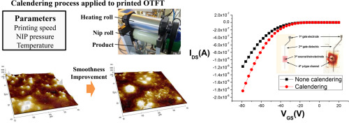
The surface roughness of a gate dielectric layer has a large effect on the electrical performance of a printed OTFT (Organic Thin Film Transistor). In this study, a treatment process called calendering is proposed to improve the electrical performance of a printed OTFT by reducing the surface roughness of the gate dielectric layer. Bottom-gate, bottom-contact structural p-type OTFT samples were fabricated by gravure printing (gate electrode and gate dielectric), inkjet printing (source/drain electrodes), and spin coating (p-type channel). Various calendering process conditions composed of temperature, speed, and nip pressure were applied in the fabrication process. Then the calendering process was optimized using the grey-based Taguchi method. For validation of the proposed method, surface roughness of the gate dielectric layer and electrical performance of the non-calendered and calendered OTFT samples were compared and analyzed. The experimental results show a significant improvement that is a 15.92% decrease in the surface roughness, a 15.46% increase in the on-off ratio, and a 30.50% increase in the field-effect mobility.
中文翻译:
通过优化压延工艺来增强印刷有机薄膜晶体管的电性能
栅极介电层的表面粗糙度对印刷的OTFT(有机薄膜晶体管)的电性能有很大的影响。在这项研究中,提出了一种称为压延的处理工艺,以通过降低栅极介电层的表面粗糙度来提高印刷OTFT的电性能。底栅,底接触结构的p型OTFT样品是通过凹版印刷(栅电极和栅电介质),喷墨印刷(源/漏电极)和旋涂(p型沟道)制成的。在制造过程中应用了由温度,速度和压区压力组成的各种压延过程条件。然后使用基于灰色的Taguchi方法优化压光过程。为了验证所提出的方法,比较和分析了未压延和压延的OTFT样品的栅极介电层的表面粗糙度和电性能。实验结果表明,表面粗糙度显着改善,表面粗糙度降低了15.92%,开关比增加了15.46%,场效应迁移率增加了30.50%。


 京公网安备 11010802027423号