当前位置:
X-MOL 学术
›
ACS Photonics
›
论文详情
Our official English website, www.x-mol.net, welcomes your
feedback! (Note: you will need to create a separate account there.)
Si-Based GeSn Lasers with Wavelength Coverage of 2–3 μm and Operating Temperatures up to 180 K
ACS Photonics ( IF 6.5 ) Pub Date : 2017-12-15 00:00:00 , DOI: 10.1021/acsphotonics.7b00938 Joe Margetis 1 , Sattar Al-Kabi 2 , Wei Du 3, 4 , Wei Dou 2 , Yiyin Zhou 2, 5 , Thach Pham 2, 5 , Perry Grant 2, 5 , Seyed Ghetmiri 2 , Aboozar Mosleh 2 , Baohua Li 5 , Jifeng Liu 6 , Greg Sun 7 , Richard Soref 7 , John Tolle 1 , Mansour Mortazavi 3 , Shui-Qing Yu 2
ACS Photonics ( IF 6.5 ) Pub Date : 2017-12-15 00:00:00 , DOI: 10.1021/acsphotonics.7b00938 Joe Margetis 1 , Sattar Al-Kabi 2 , Wei Du 3, 4 , Wei Dou 2 , Yiyin Zhou 2, 5 , Thach Pham 2, 5 , Perry Grant 2, 5 , Seyed Ghetmiri 2 , Aboozar Mosleh 2 , Baohua Li 5 , Jifeng Liu 6 , Greg Sun 7 , Richard Soref 7 , John Tolle 1 , Mansour Mortazavi 3 , Shui-Qing Yu 2
Affiliation
|
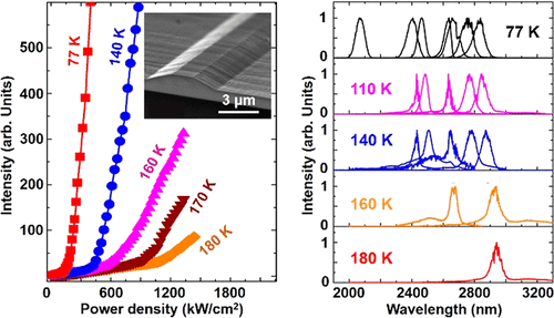
A Si-based monolithic laser is strongly desired for the full integration of Si-photonics. Lasing from the direct bandgap group-IV GeSn alloy has opened a new avenue, different from the hybrid III–V-on-Si integration approach. We demonstrated optically pumped GeSn lasers on Si with broad wavelength coverage from 2 to 3 μm. The GeSn alloys were grown using newly developed approaches with an industry standard chemical vapor deposition reactor and low-cost commercially available precursors. The achieved maximum Sn composition of 17.5% exceeded the generally acknowledged Sn incorporation limits found with similar deposition chemistries. The highest lasing temperature was measured as 180 K with the active layer thickness as thin as 260 nm. The unprecedented lasing performance is mainly due to the unique growth approaches, which offer high-quality epitaxial materials. The results reported in this work show a major advance toward Si-based mid-infrared laser sources for integrated photonics.
中文翻译:

硅基GeSn激光器,波长覆盖范围为2–3μm,工作温度高达180 K
完全集成硅光子学非常需要基于硅的单片激光器。直接带隙IV族GeSn合金的发射开辟了一条新的途径,不同于III-V-on-Si混合集成方法。我们在Si上演示了光泵浦GeSn激光器,其波长覆盖范围从2到3μm。GeSn合金是使用最新开发的方法与行业标准的化学气相沉积反应器和低成本的商用前体一起生长的。达到的最大Sn成分为17.5%,超过了相似沉积化学方法中公认的Sn掺入极限。测得的最高激光发射温度为180 K,而有源层的厚度则薄至260 nm。前所未有的激光性能主要归功于独特的增长方式,提供高质量的外延材料。这项工作报告的结果表明,集成光子学在基于硅的中红外激光源方面取得了重大进展。
更新日期:2017-12-15
中文翻译:
硅基GeSn激光器,波长覆盖范围为2–3μm,工作温度高达180 K
完全集成硅光子学非常需要基于硅的单片激光器。直接带隙IV族GeSn合金的发射开辟了一条新的途径,不同于III-V-on-Si混合集成方法。我们在Si上演示了光泵浦GeSn激光器,其波长覆盖范围从2到3μm。GeSn合金是使用最新开发的方法与行业标准的化学气相沉积反应器和低成本的商用前体一起生长的。达到的最大Sn成分为17.5%,超过了相似沉积化学方法中公认的Sn掺入极限。测得的最高激光发射温度为180 K,而有源层的厚度则薄至260 nm。前所未有的激光性能主要归功于独特的增长方式,提供高质量的外延材料。这项工作报告的结果表明,集成光子学在基于硅的中红外激光源方面取得了重大进展。


 京公网安备 11010802027423号