npj Flexible Electronics ( IF 12.3 ) Pub Date : 2017-12-13 , DOI: 10.1038/s41528-017-0013-x Miki Trifunovic , Paolo Maria Sberna , Tatsuya Shimoda , Ryoichi Ishihara
|
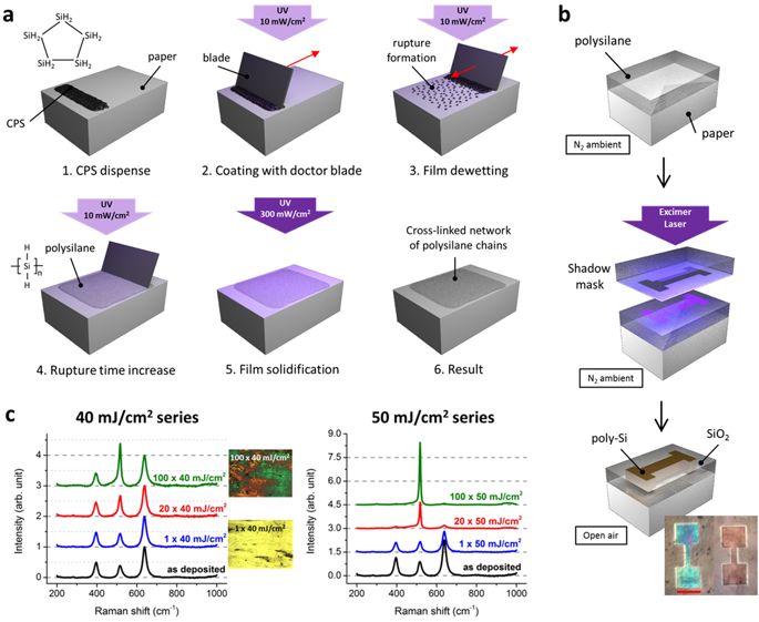
Printing of electronics is pursued as a low-cost alternative to conventional manufacturing processes. In addition, owing to relatively low process temperatures, flexible substrates can be used enabling novel applications. Among flexible substrates, paper was found to be a particularly interesting candidate, since it has an order of magnitude lower price than low-cost polymer alternatives, and is biodegradable. As ink materials, organic and metal-oxide semiconductors are thoroughly being investigated; however, they lack in electric performance compared to silicon in terms of device mobility, reliability, and energy efficiency. In recent years, liquid precursors for silicon were found and used to create polycrystalline silicon (poly-Si). However, fabrication of transistors on top of low-cost flexible substrates such as paper has remained an outstanding challenge. Here we demonstrate both p-channel and n-channel poly-Si thin-film transistors (TFTs) fabricated directly on top of paper with field-effect mobilities of 6.2 and 2.0 cm2/V s, respectively. Many fabrication challenges have been overcome by limiting the maximum process temperature to approximately 100 °C, and avoiding liquid chemicals commonly used for etching and cleaning. Patterning of poly-Si has been achieved by additive selective crystallization of the precursor film using an excimer laser. This work serves as a proof of concept, and has the potential to further improve device performance. Owing to the low-cost, biodegradable nature of paper, and the high performance, reliability, and energy efficiency of poly-Si TFTs, this work opens a pathway toward truly low-cost, low-power, recyclable applications including smart packages, biodegradable health monitoring units, flexible displays, and disposable sensor nodes.
中文翻译:
在纸质基板上生产的基于溶液的多晶硅晶体管
电子印刷被认为是传统制造工艺的低成本替代品。另外,由于相对较低的处理温度,可以使用柔性基板以实现新颖的应用。在柔性基材中,发现纸张是特别有趣的候选材料,因为它的价格比低成本的聚合物替代品低一个数量级,并且可以生物降解。作为油墨材料,有机和金属氧化物半导体已得到了深入研究。然而,就器件移动性,可靠性和能效而言,它们在电性能上不如硅。近年来,发现了硅的液体前体,并用于制造多晶硅(poly-Si)。然而,在诸如纸之类的低成本柔性衬底上制造晶体管仍然是一项艰巨的挑战。在这里,我们演示了直接在纸上制造的p沟道和n沟道多晶硅薄膜晶体管(TFT),其场效应迁移率分别为6.2和2.0 cm2 / V s分别。通过将最高工艺温度限制在大约100°C,避免使用通常用于蚀刻和清洁的液体化学品,克服了许多制造难题。多晶硅的图案化是通过使用准分子激光器对前体膜进行附加选择性结晶来实现的。这项工作可作为概念证明,并有可能进一步提高设备性能。由于纸张的低成本,可生物降解的特性以及多晶硅TFT的高性能,可靠性和能效,这项工作为通往真正的低成本,低功耗,可回收应用(包括智能包装,可生物降解的应用)开辟了道路。健康监控单元,柔性显示器和一次性传感器节点。


 京公网安备 11010802027423号