Our official English website, www.x-mol.net, welcomes your feedback! (Note: you will need to create a separate account there.)
Optical pumped InGaAs/GaAs nano-ridge laser epitaxially grown on a standard 300-mm Si wafer
Optica ( IF 10.4 ) Pub Date : 2017-11-29 , DOI: 10.1364/optica.4.001468 Yuting Shi , Zhechao Wang , Joris Van Campenhout , Marianna Pantouvaki , Weiming Guo , Bernardette Kunert , Dries Van Thourhout
Optica ( IF 10.4 ) Pub Date : 2017-11-29 , DOI: 10.1364/optica.4.001468 Yuting Shi , Zhechao Wang , Joris Van Campenhout , Marianna Pantouvaki , Weiming Guo , Bernardette Kunert , Dries Van Thourhout
|
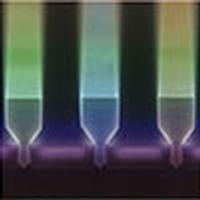
Fully exploiting the potential of silicon photonics requires high-performance active devices such as lasers, which can be monolithically integrated in a scalable way. However, direct bandgap III–V semiconductors exhibit a large lattice mismatch and/or strongly differing thermal expansion coefficient with silicon. This makes monolithic integration on silicon without introducing excessive defects in the material extremely difficult. The majority of the methods proposed thus far either are not compatible with further low-cost integration or rely on a special substrate. Here we demonstrate monolithic InGaAs/GaAs single-mode nano-ridge lasers directly grown on a standard (001) 300-mm Si wafer. Exploiting the aspect ratio defect trapping technique, unwanted defects are confined to a narrow trench defined in the silicon substrate. The nano-ridge structures subsequently grown out of these trenches are of high crystalline quality as shown by high-resolution transmission electron microscopy analysis and a strong photoluminescence response. They can be controlled in shape by optimizing the growth conditions, which allows us to minimize substrate leakage and maximize confinement in the InGaAs quantum wells providing optical gain. Distributed feedback lasers were fabricated by defining a first-order grating in the nano-ridge. Under pulsed optical pumping, single-mode lasing with side mode suppression over 28 dB was shown, and precise control of the emission wavelength over 60 nm was achieved. This demonstration proves the high quality of the material and provides a credible road towards a CMOS-compatible platform for high-volume manufacturing of silicon photonic integrated circuits, including laser and amplifier devices.
中文翻译:

在标准300mm Si晶片上外延生长的光泵浦InGaAs / GaAs纳米脊激光器
要充分利用硅光子学的潜力,就需要高性能有源器件,例如激光器,它们可以以可扩展的方式单片集成。但是,直接带隙III–V半导体表现出较大的晶格失配和/或与硅的热膨胀系数差异很大。这使得在硅上进行单片集成而又不会在材料中引入过多的缺陷非常困难。迄今为止,提出的大多数方法要么与进一步的低成本集成不兼容,要么依赖于特殊的基板。在这里,我们展示了直接在标准(001)300毫米Si晶圆上生长的单片InGaAs / GaAs单模纳米脊激光器。利用长宽比缺陷捕获技术,不需要的缺陷被限制在硅衬底中限定的狭窄沟槽中。随后从这些沟槽中生长出来的纳米脊结构具有很高的晶体质量,如高分辨率透射电子显微镜分析所显示的那样,并且具有很强的光致发光响应。可以通过优化生长条件来控制它们的形状,这使我们能够最大程度地减少衬底泄漏并最大程度地限制提供光增益的InGaAs量子阱。通过在纳米脊中定义一阶光栅来制造分布式反馈激光器。在脉冲光泵浦下,显示了具有超过28 dB的边模抑制的单模激光,并且可以精确控制60 nm以上的发射波长。
更新日期:2017-12-20
中文翻译:
在标准300mm Si晶片上外延生长的光泵浦InGaAs / GaAs纳米脊激光器
要充分利用硅光子学的潜力,就需要高性能有源器件,例如激光器,它们可以以可扩展的方式单片集成。但是,直接带隙III–V半导体表现出较大的晶格失配和/或与硅的热膨胀系数差异很大。这使得在硅上进行单片集成而又不会在材料中引入过多的缺陷非常困难。迄今为止,提出的大多数方法要么与进一步的低成本集成不兼容,要么依赖于特殊的基板。在这里,我们展示了直接在标准(001)300毫米Si晶圆上生长的单片InGaAs / GaAs单模纳米脊激光器。利用长宽比缺陷捕获技术,不需要的缺陷被限制在硅衬底中限定的狭窄沟槽中。随后从这些沟槽中生长出来的纳米脊结构具有很高的晶体质量,如高分辨率透射电子显微镜分析所显示的那样,并且具有很强的光致发光响应。可以通过优化生长条件来控制它们的形状,这使我们能够最大程度地减少衬底泄漏并最大程度地限制提供光增益的InGaAs量子阱。通过在纳米脊中定义一阶光栅来制造分布式反馈激光器。在脉冲光泵浦下,显示了具有超过28 dB的边模抑制的单模激光,并且可以精确控制60 nm以上的发射波长。


 京公网安备 11010802027423号