当前位置:
X-MOL 学术
›
Prog. Photovoltaics
›
论文详情
Our official English website, www.x-mol.net, welcomes your
feedback! (Note: you will need to create a separate account there.)
Double band gap gradients in sequentially processed photovoltaic absorbers from the Cu(In,Ga)Se2‐ZnSe pseudobinary system
Progress in Photovoltaics ( IF 8.0 ) Pub Date : 2017-11-08 , DOI: 10.1002/pip.2958 Rokas Kondrotas 1 , Florian Oliva 1 , Xavier Alcobe 2 , Victor Izquierdo-Roca 1 , Alejandro Perez-Rodriguez 1, 3 , Edgardo Saucedo 1 , Paul Pistor 1, 4
Progress in Photovoltaics ( IF 8.0 ) Pub Date : 2017-11-08 , DOI: 10.1002/pip.2958 Rokas Kondrotas 1 , Florian Oliva 1 , Xavier Alcobe 2 , Victor Izquierdo-Roca 1 , Alejandro Perez-Rodriguez 1, 3 , Edgardo Saucedo 1 , Paul Pistor 1, 4
Affiliation
|
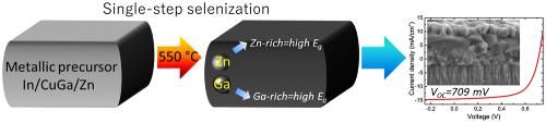
Wide band gap Cu(In,Ga)Se2‐ZnSe (CIGZSe) thin films have been synthesized using a sequential process, with the objective to demonstrate the possibility to tune the band gap and introduce double gradients playing with the content of Ga at the back and Zn at the front. In a first approach, we start by varying the 3‐valent cationic composition of the system, and then we modify the reactive annealing conditions in order to understand and control the elemental gradients. Structural, compositional, and morphological properties of the corresponding absorbers were analysed by X‐ray diffraction, Raman spectroscopy, energy dispersive spectrometer, Auger spectroscopy, and scanning electron microscopy. Solar cells were fabricated and characterized, focusing on the identification of the most promising cationic composition. The compounds from the complex Cu(In,Ga)Se2‐ZnSe system can adopt either the chalcopyrite or sphalerite phases depending on the [Zn]/[metals] and [Ga]/([Ga] + [In]) ratios. We demonstrate that Ga naturally diffuses towards the back region forming a Ga‐rich, wide band gap chalcopyrite phase at the rear contact, as is commonly observed for a Cu(In,Ga)Se2 synthesized via selenization process. On the contrary, Zn is preferably accumulated at the surface, forming wide band gap sphalerite Cu(In,Ga)ZnSe3 phases with high Zn and very low Ga contents at the surface. This opens an additional way to control the surface's band gap. With this approach, the formation of a doubly graded band gap profile with Ga‐rich layers at the back and Zn‐rich layers at the front is demonstrated in a single selenization step, showing promising efficiency and open circuit voltage values (up to 6.7% and 709 mV, respectively).
中文翻译:

Cu(In,Ga)Se2-ZnSe伪二元体系相继处理的光伏吸收体中的双带隙梯度
宽带隙Cu(In,Ga)Se 2‐ZnSe(CIGZSe)薄膜是使用顺序过程合成的,目的是证明可以调谐带隙并引入双重梯度的可能性,其中背面的Ga和正面的Zn含量较高。在第一种方法中,我们首先更改系统的三价阳离子组成,然后修改反应性退火条件,以了解和控制元素梯度。通过X射线衍射,拉曼光谱,能量色散光谱仪,俄歇光谱和扫描电子显微镜分析了相应吸收体的结构,组成和形态特性。制造并表征了太阳能电池,着眼于最有前途的阳离子成分的鉴定。复杂的Cu(In,Ga)Se化合物2 ZnSe体系可以采用黄铜矿或闪锌矿相,具体取决于[Zn] / [金属]和[Ga] /([Ga] + [In])的比例。我们证明了Ga自然地向后方扩散,在后部接触处形成了富含Ga的宽带隙黄铜矿相,这是通过硒化过程合成的Cu(In,Ga)Se 2的常见现象。相反,Zn优选在表面蓄积,形成宽带隙闪锌矿Cu(In,Ga)ZnSe 3。表面具有高Zn和极低Ga含量的相。这为控制表面的带隙开辟了另一种方式。通过这种方法,在一个硒化步骤中就证明了形成了一个双梯度带隙轮廓,在背面具有富Ga层,在正面具有富Zn层,显示出有希望的效率和开路电压值(高达6.7%)和709 mV)。
更新日期:2017-11-08
中文翻译:
Cu(In,Ga)Se2-ZnSe伪二元体系相继处理的光伏吸收体中的双带隙梯度
宽带隙Cu(In,Ga)Se 2‐ZnSe(CIGZSe)薄膜是使用顺序过程合成的,目的是证明可以调谐带隙并引入双重梯度的可能性,其中背面的Ga和正面的Zn含量较高。在第一种方法中,我们首先更改系统的三价阳离子组成,然后修改反应性退火条件,以了解和控制元素梯度。通过X射线衍射,拉曼光谱,能量色散光谱仪,俄歇光谱和扫描电子显微镜分析了相应吸收体的结构,组成和形态特性。制造并表征了太阳能电池,着眼于最有前途的阳离子成分的鉴定。复杂的Cu(In,Ga)Se化合物2 ZnSe体系可以采用黄铜矿或闪锌矿相,具体取决于[Zn] / [金属]和[Ga] /([Ga] + [In])的比例。我们证明了Ga自然地向后方扩散,在后部接触处形成了富含Ga的宽带隙黄铜矿相,这是通过硒化过程合成的Cu(In,Ga)Se 2的常见现象。相反,Zn优选在表面蓄积,形成宽带隙闪锌矿Cu(In,Ga)ZnSe 3。表面具有高Zn和极低Ga含量的相。这为控制表面的带隙开辟了另一种方式。通过这种方法,在一个硒化步骤中就证明了形成了一个双梯度带隙轮廓,在背面具有富Ga层,在正面具有富Zn层,显示出有希望的效率和开路电压值(高达6.7%)和709 mV)。


 京公网安备 11010802027423号