当前位置:
X-MOL 学术
›
Chem. Mater.
›
论文详情
Our official English website, www.x-mol.net, welcomes your
feedback! (Note: you will need to create a separate account there.)
Influence of the Contact Area on the Current Density across Molecular Tunneling Junctions Measured with EGaIn Top-Electrodes
Chemistry of Materials ( IF 7.2 ) Pub Date : 2017-12-21 00:00:00 , DOI: 10.1021/acs.chemmater.7b03384 Philipp Rothemund 1, 2, 3 , Carleen Morris Bowers 2 , Zhigang Suo 1, 3 , George M. Whitesides 2, 3, 4
Chemistry of Materials ( IF 7.2 ) Pub Date : 2017-12-21 00:00:00 , DOI: 10.1021/acs.chemmater.7b03384 Philipp Rothemund 1, 2, 3 , Carleen Morris Bowers 2 , Zhigang Suo 1, 3 , George M. Whitesides 2, 3, 4
Affiliation
|
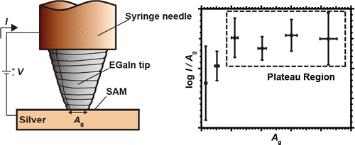
This paper describes the relationship between the rates of charge transport (by tunneling) across self-assembled monolayers (SAMs) in a metal/SAM//Ga2O3/EGaIn junction and the geometric contact area (Ag) between the conical Ga2O3/EGaIn top-electrode and the bottom-electrode. Measurements of current density, J(V), across SAMs of decanethiolate on silver demonstrate that J(V) increases with Ag when the contact area is small (Ag < 1000 μm2), but reaches a plateau between 1000 and 4000 μm2, where J(0.5 V) ≈ 10–0.52±0.10 A/cm2. The method used to fabricate Ga2O3/EGaIn electrodes generates a tip whose apex is thicker and rougher than its thin, smoother sides. When Ag is small, the Ga2O3/EGaIn electrode contacts the bottom-electrode principally over this rough apex and forms irreproducible areas of electrical contact. When Ag is large, the contact is through the smoother regions peripheral to the apex and is much more reproducible. Measurements of contact pressure between conical EGaIn electrodes and atomic force microscope cantilevers demonstrate that the nominal contact pressure (governed by the mechanical behavior of the oxide skin) decreases approximately inversely with the diameter of geometric contact. This self-regulation of pressure prevents damage to the SAM and makes the ratio of electrical contact area to geometric footprint approximately constant.
中文翻译:

接触面积对通过EGaIn上电极测量的分子隧穿结上电流密度的影响
本文描述了金属/ SAM // Ga 2 O 3 / EGaIn结中自组装单分子层(SAMs)上的电荷传输速率(通过隧穿)与锥形Ga之间的几何接触面积(A g)之间的关系。2 O 3 / EGaIn顶部电极和底部电极。电流密度的测量,Ĵ(V),跨越上银decanethiolate的自组装膜证明Ĵ(V带)的增加甲克时的接触面积是小的(甲克<1000微米2),但达到1000至4000微米之间的高原2,其中J(0.5 V)≈10 –0.52±0.10 A / cm 2。用于制造Ga 2 O 3 / EGaIn电极的方法产生的尖端比其薄而光滑的侧面的尖端更厚且更粗糙。当A g较小时,Ga 2 O 3 / EGaIn电极主要在该粗糙顶点上接触底部电极,并形成不可复制的电接触区域。当A g如果接触角大,则接触是通过顶点周围较平滑的区域进行的,并且可重现性更高。锥形EGaIn电极和原子力显微镜悬臂之间的接触压力的测量结果表明,名义接触压力(由氧化皮的机械性能控制)与几何接触直径成反比地减小。压力的这种自我调节可防止损坏SAM,并使电接触面积与几何尺寸的比值近似恒定。
更新日期:2017-12-21
中文翻译:
接触面积对通过EGaIn上电极测量的分子隧穿结上电流密度的影响
本文描述了金属/ SAM // Ga 2 O 3 / EGaIn结中自组装单分子层(SAMs)上的电荷传输速率(通过隧穿)与锥形Ga之间的几何接触面积(A g)之间的关系。2 O 3 / EGaIn顶部电极和底部电极。电流密度的测量,Ĵ(V),跨越上银decanethiolate的自组装膜证明Ĵ(V带)的增加甲克时的接触面积是小的(甲克<1000微米2),但达到1000至4000微米之间的高原2,其中J(0.5 V)≈10 –0.52±0.10 A / cm 2。用于制造Ga 2 O 3 / EGaIn电极的方法产生的尖端比其薄而光滑的侧面的尖端更厚且更粗糙。当A g较小时,Ga 2 O 3 / EGaIn电极主要在该粗糙顶点上接触底部电极,并形成不可复制的电接触区域。当A g如果接触角大,则接触是通过顶点周围较平滑的区域进行的,并且可重现性更高。锥形EGaIn电极和原子力显微镜悬臂之间的接触压力的测量结果表明,名义接触压力(由氧化皮的机械性能控制)与几何接触直径成反比地减小。压力的这种自我调节可防止损坏SAM,并使电接触面积与几何尺寸的比值近似恒定。


 京公网安备 11010802027423号