当前位置:
X-MOL 学术
›
Adv. Electron. Mater.
›
论文详情
Our official English website, www.x-mol.net, welcomes your
feedback! (Note: you will need to create a separate account there.)
Controlled Low‐Frequency Electrical Noise of Monolayer MoS2 with Ohmic Contact and Tunable Carrier Concentration
Advanced Electronic Materials ( IF 5.3 ) Pub Date : 2017-12-05 , DOI: 10.1002/aelm.201700340 Ji-Wun Wang,Yen-Po Liu,Po-Han Chen,Meng-Hsi Chuang,Atiye Pezeshki,Dah-Chin Ling,Jeng-Chung Chen,Yung-Fu Chen,Yi-Hsien Lee
Advanced Electronic Materials ( IF 5.3 ) Pub Date : 2017-12-05 , DOI: 10.1002/aelm.201700340 Ji-Wun Wang,Yen-Po Liu,Po-Han Chen,Meng-Hsi Chuang,Atiye Pezeshki,Dah-Chin Ling,Jeng-Chung Chen,Yung-Fu Chen,Yi-Hsien Lee
|
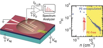
Semiconducting monolayers of transition metal dichalcogenides (TMDs) are considered as emergent materials for nanodevices and optoelectronic applications. The low‐frequency electrical noise of TMD‐based devices is much higher than Si and other conventional semiconductors. The reduction of this noise along with control of the Ohmic contact and carrier concentration of the such devices remain major challenges. Here, the low‐frequency (1/f) noise and transport properties of chemical‐vapor‐deposition‐grown MoS2 are presented. The high mobility of 20–40 cm2 V−1 s−1 of the monolayer devices is highly reproducible. Reliable methods to induce Ohmic contact and to tune carrier density over a wide range of 1011–1014 cm−2 are presented to study the fundamental mechanism of the 1/f noise. The noise performance in the high carrier concentration regime is explored for the first time with Ohmic contact of the devices and ideal sample quality. A significant reduction of the noise figure of merit is achievable in the high‐density regime. Polymer electrolyte encapsulation provides a practical method to effectively tune carrier density and engineer surface trap states of the monolayer TMDs, which would be helpful for practical applications of 2D atomic layers in nanoelectronics and photonics.
中文翻译:

具有欧姆接触和可调载流子浓度的单层MoS2的受控低频电噪声
过渡金属二硫化碳(TMD)的半导体单层被认为是用于纳米器件和光电应用的新兴材料。基于TMD的器件的低频电噪声要比Si和其他常规半导体高得多。降低这种噪声以及控制此类器件的欧姆接触和载流子浓度仍然是主要挑战。在此,介绍了化学气相沉积生长的MoS 2的低频(1 / f)噪声和传输特性。单层器件的20–40 cm 2 V -1 s -1的高迁移率具有很高的再现性。可靠的诱导欧姆接触并在10的宽范围内调节载流子密度的方法提出了11 – 10 14 cm -2来研究1 / f噪声的基本机理。通过设备的欧姆接触和理想的样品质量,首次探索了高载流子浓度条件下的噪声性能。在高密度条件下,可以显着降低噪声品质因数。聚合物电解质的封装提供了一种实用的方法,可以有效地调整载流子密度和设计单层TMD的表面陷阱状态,这将有助于2D原子层在纳米电子学和光子学中的实际应用。
更新日期:2017-12-05
中文翻译:
具有欧姆接触和可调载流子浓度的单层MoS2的受控低频电噪声
过渡金属二硫化碳(TMD)的半导体单层被认为是用于纳米器件和光电应用的新兴材料。基于TMD的器件的低频电噪声要比Si和其他常规半导体高得多。降低这种噪声以及控制此类器件的欧姆接触和载流子浓度仍然是主要挑战。在此,介绍了化学气相沉积生长的MoS 2的低频(1 / f)噪声和传输特性。单层器件的20–40 cm 2 V -1 s -1的高迁移率具有很高的再现性。可靠的诱导欧姆接触并在10的宽范围内调节载流子密度的方法提出了11 – 10 14 cm -2来研究1 / f噪声的基本机理。通过设备的欧姆接触和理想的样品质量,首次探索了高载流子浓度条件下的噪声性能。在高密度条件下,可以显着降低噪声品质因数。聚合物电解质的封装提供了一种实用的方法,可以有效地调整载流子密度和设计单层TMD的表面陷阱状态,这将有助于2D原子层在纳米电子学和光子学中的实际应用。


 京公网安备 11010802027423号