当前位置:
X-MOL 学术
›
Chem. Mater.
›
论文详情
Our official English website, www.x-mol.net, welcomes your
feedback! (Note: you will need to create a separate account there.)
Alignment of Redox Levels at Semiconductor–Water Interfaces
Chemistry of Materials ( IF 7.2 ) Pub Date : 2017-12-21 00:00:00 , DOI: 10.1021/acs.chemmater.7b02619 Zhendong Guo 1 , Francesco Ambrosio 1 , Wei Chen 1, 2 , Patrick Gono 1 , Alfredo Pasquarello 1
Chemistry of Materials ( IF 7.2 ) Pub Date : 2017-12-21 00:00:00 , DOI: 10.1021/acs.chemmater.7b02619 Zhendong Guo 1 , Francesco Ambrosio 1 , Wei Chen 1, 2 , Patrick Gono 1 , Alfredo Pasquarello 1
Affiliation
|
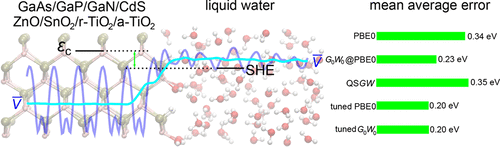
We determine the band alignment between various semiconductors and liquid water by combining molecular dynamics (MD) simulations of atomistic interface models, electronic-structure calculations at the hybrid-functional and GW level, and a computational standard hydrogen electrode. Our study comprises GaAs, GaP, GaN, CdS, ZnO, SnO2, rutile TiO2, and anatase TiO2. For each semiconductor, we generate atomistic interface models with liquid water at the pH corresponding to the point of zero charge. The molecular dynamics are started from two kinds of initial configurations, in which the water molecules are either molecularly (m) or dissociatively (d) adsorbed on the semiconductor surface. The calculated band offsets are found to be strongly influenced by the adsorption mode at the semiconductor–water interface, leading to differences larger than 1 eV between m and d models of the same semiconductor. We first assess the accuracy of various ab initio electronic-structure schemes. The use of a standard hybrid functional leads to large errors for the conduction band edge but nevertheless accounts accurately for the position of the valence band edge. One-shot GW calculations with a starting point at the semilocal density functional level do not yield any improvement. It is necessary to turn to one-shot GW calculations based on a hybrid-functional starting point to achieve a noticeable improvement in the determination of the band edges, with mean average errors ranging between 0.23 and 0.27 eV. The use of state-of-the-art quasiparticle self-consistent GW schemes does not lead to any further improvement for the set of semiconductors under investigation. Further improvement with mean average errors of 0.20 eV is obtained when turning to hybrid-functional and GW methods, in which the experimental band gap of the semiconductor is enforced by construction. The present work sets a benchmark for the accuracy by which band edges at semiconductor–water interfaces can be obtained with current advanced electronic-structure methods. In particular, the importance of providing an atomistic description of the semiconductor–water interface is emphasized.
中文翻译:

半导体-水界面处氧化还原水平的对齐
我们通过结合原子界面模型的分子动力学(MD)模拟,混合功能和GW级的电子结构计算以及计算标准氢电极,确定各种半导体与液态水之间的能带对准。我们的研究包括GaAs,GaP,GaN,CdS,ZnO,SnO 2,金红石TiO 2和锐钛矿TiO 2。对于每种半导体,我们使用与零电荷点相对应的pH值的液态水生成原子界面模型。分子动力学从两种初始构型开始,其中水分子要么是分子(m)要么是解离性(d)吸附在半导体表面上。发现计算出的带偏移受半导体-水界面处的吸附模式的强烈影响,导致同一半导体的m和d模型之间的差异大于1 eV 。我们首先评估各种从头开始的电子结构方案的准确性。标准混合功能的使用会导致导带边缘的较大误差,但仍能准确说明价带边缘的位置。以半局部密度函数水平为起点的单次GW计算不会产生任何改善。有必要转向一次性GW基于混合功能起点的计算可以显着改善带边缘的确定,平均平均误差在0.23和0.27 eV之间。使用最新的准粒子自洽GW方案不会对正在研究的半导体组产生任何进一步的改进。转向混合功能和GW时,平均平均误差为0.20 eV的情况得到了进一步的改进方法,其中半导体的实验带隙是通过构造来实现的。目前的工作为使用当前先进的电子结构方法可获得半导体-水界面处的能带边缘的精度设定了基准。特别是,强调了提供半导体-水界面原子描述的重要性。
更新日期:2017-12-21
中文翻译:
半导体-水界面处氧化还原水平的对齐
我们通过结合原子界面模型的分子动力学(MD)模拟,混合功能和GW级的电子结构计算以及计算标准氢电极,确定各种半导体与液态水之间的能带对准。我们的研究包括GaAs,GaP,GaN,CdS,ZnO,SnO 2,金红石TiO 2和锐钛矿TiO 2。对于每种半导体,我们使用与零电荷点相对应的pH值的液态水生成原子界面模型。分子动力学从两种初始构型开始,其中水分子要么是分子(m)要么是解离性(d)吸附在半导体表面上。发现计算出的带偏移受半导体-水界面处的吸附模式的强烈影响,导致同一半导体的m和d模型之间的差异大于1 eV 。我们首先评估各种从头开始的电子结构方案的准确性。标准混合功能的使用会导致导带边缘的较大误差,但仍能准确说明价带边缘的位置。以半局部密度函数水平为起点的单次GW计算不会产生任何改善。有必要转向一次性GW基于混合功能起点的计算可以显着改善带边缘的确定,平均平均误差在0.23和0.27 eV之间。使用最新的准粒子自洽GW方案不会对正在研究的半导体组产生任何进一步的改进。转向混合功能和GW时,平均平均误差为0.20 eV的情况得到了进一步的改进方法,其中半导体的实验带隙是通过构造来实现的。目前的工作为使用当前先进的电子结构方法可获得半导体-水界面处的能带边缘的精度设定了基准。特别是,强调了提供半导体-水界面原子描述的重要性。


 京公网安备 11010802027423号