当前位置:
X-MOL 学术
›
J. Mater. Chem. C
›
论文详情
Our official English website, www.x-mol.net, welcomes your
feedback! (Note: you will need to create a separate account there.)
Growth, characterization and optoelectronic applications of pure-phase large-area CsPb2Br5 flake single crystals†
Journal of Materials Chemistry C ( IF 5.7 ) Pub Date : 2017-11-27 00:00:00 , DOI: 10.1039/c7tc04834c Zhaojun Zhang 1, 2, 3, 4, 5 , Yanming Zhu 1, 2, 3, 4, 5 , Weiliang Wang 1, 2, 3, 4, 5 , Wei Zheng 2, 3, 4, 5, 6 , Richeng Lin 1, 2, 3, 4, 5 , Feng Huang 2, 3, 4, 5, 6
Journal of Materials Chemistry C ( IF 5.7 ) Pub Date : 2017-11-27 00:00:00 , DOI: 10.1039/c7tc04834c Zhaojun Zhang 1, 2, 3, 4, 5 , Yanming Zhu 1, 2, 3, 4, 5 , Weiliang Wang 1, 2, 3, 4, 5 , Wei Zheng 2, 3, 4, 5, 6 , Richeng Lin 1, 2, 3, 4, 5 , Feng Huang 2, 3, 4, 5, 6
Affiliation
|
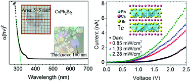
To clarify the controversies on CsPb2Br5 and extend its optoelectronic applications, from a thermodynamic equilibrium growth system, pure phase high quality CsPb2Br5 single crystals (maximum area: 5 × 5 mm2, minimum thickness: 160 nm) were successfully obtained. Optical characterization results indicated a 3.87 eV bandgap for CsPb2Br5, clarifying the controversies on CsPb2Br5. The fabricated photodetector showed a sensitive and fast deep-UV photoresponse, demonstrating the potential applications of CsPb2Br5 in deep-UV detection. Theoretical calculations suggested that the wide bandgap of CsPb2Br5 resulted from its layered structure and short Pb–Br bonds.
中文翻译:

纯相大面积CsPb 2 Br 5片状单晶的生长,表征和光电应用†
为了阐明关于CsPb 2 Br 5的争议并扩展其光电应用,从热力学平衡生长系统成功地获得了纯相高质量CsPb 2 Br 5单晶(最大面积:5×5 mm 2,最小厚度:160 nm)。获得。光学表征结果表明CsPb 2 Br 5的带隙为3.87 eV ,从而澄清了CsPb 2 Br 5的争议。制成的光电探测器显示出灵敏且快速的深紫外光响应,证明了CsPb 2 Br 5的潜在应用在深紫外线检测中。理论计算表明,CsPb 2 Br 5的带隙宽是由于其层状结构和短的Pb-Br键所致。
更新日期:2017-11-27
中文翻译:
纯相大面积CsPb 2 Br 5片状单晶的生长,表征和光电应用†
为了阐明关于CsPb 2 Br 5的争议并扩展其光电应用,从热力学平衡生长系统成功地获得了纯相高质量CsPb 2 Br 5单晶(最大面积:5×5 mm 2,最小厚度:160 nm)。获得。光学表征结果表明CsPb 2 Br 5的带隙为3.87 eV ,从而澄清了CsPb 2 Br 5的争议。制成的光电探测器显示出灵敏且快速的深紫外光响应,证明了CsPb 2 Br 5的潜在应用在深紫外线检测中。理论计算表明,CsPb 2 Br 5的带隙宽是由于其层状结构和短的Pb-Br键所致。


 京公网安备 11010802027423号