当前位置:
X-MOL 学术
›
CrystEngComm
›
论文详情
Our official English website, www.x-mol.net, welcomes your
feedback! (Note: you will need to create a separate account there.)
Seed-mediated phase-selective growth of Cu2GeS3 hollow nanoparticles with huge cavities
CrystEngComm ( IF 2.6 ) Pub Date : 2017-09-12 00:00:00 , DOI: 10.1039/c7ce01503h Chunwei Dong 1, 2, 3, 4, 5 , Rui Ge 1, 2, 3, 4, 5 , Dong Yao 1, 2, 3, 4, 5 , Zhennan Wu 1, 2, 3, 4, 5 , Zidong Wang 1, 2, 3, 4, 5 , Yi Liu 1, 2, 3, 4, 5 , Bai Yang 1, 2, 3, 4, 5 , Hao Zhang 1, 2, 3, 4, 5
CrystEngComm ( IF 2.6 ) Pub Date : 2017-09-12 00:00:00 , DOI: 10.1039/c7ce01503h Chunwei Dong 1, 2, 3, 4, 5 , Rui Ge 1, 2, 3, 4, 5 , Dong Yao 1, 2, 3, 4, 5 , Zhennan Wu 1, 2, 3, 4, 5 , Zidong Wang 1, 2, 3, 4, 5 , Yi Liu 1, 2, 3, 4, 5 , Bai Yang 1, 2, 3, 4, 5 , Hao Zhang 1, 2, 3, 4, 5
Affiliation
|
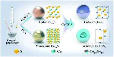
Although significant progress has been achieved in the synthesis of hollow nanoparticles (NPs), research on copper-based multinary chalcogenide (CMC) semiconductor NPs with hollow structures is still less developed. In this work, we demonstrate an effective method for the phase-selective synthesis of cubic Cu2GeS3 hollow NPs (HNPs) with huge cavities and thin shells. This method includes the nucleation of Cu2−xS seeds, followed by unequal diffusion between Cu+ and Ge4+. A common rule for the phase-selective growth of CMC NPs has been revealed: the nucleation step is the crystal phase-determining step in the growth process of CMC NPs, and the sulfur sources govern the crystal phase of the nucleus. Because of their huge cavities, the as-prepared large Cu2GeS3 HNPs are proved to be macroporous materials with a specific surface area of 22.1 m2 g−1. Besides, cubic Cu2GeS3 HNPs with small cavities are also synthesized, following the same method with little modification. By integrating the advantages of the large Cu2GeS3 HNPs (high surface-to-volume area) and the small Cu2GeS3 HNPs (good dispersibility and monodispersity), a new kind of two-layer photoelectrode is prepared. Compared with the photoelectrodes prepared using pure large and small Cu2GeS3 HNPs, the two-layer photoelectrode exhibits superior performance for photoelectrochemistry due to the high interface area of the upper layer and the ideal compactness of the bottom layer.
中文翻译:

巨大介孔的Cu 2 GeS 3空心纳米粒子的种子介导相选择生长
尽管在空心纳米颗粒(NPs)的合成方面已取得重大进展,但对具有空心结构的铜基多元硫族化物(CMC)半导体NP的研究仍很少。在这项工作中,我们证明了一种有效的方法用于相选择合成具有大孔洞和薄壳的立方Cu 2 GeS 3空心NP(HNP)。该方法包括Cu 2- x S晶核的成核,然后Cu +和Ge 4+之间的扩散不均等。已经揭示了CMC NPs相选择生长的一个通用规则:成核步骤是CMC NPs生长过程中的晶体相确定步骤,硫源控制着原子核的晶相。由于其巨大的空腔,所制备的大Cu 2 GeS 3 HNP被证明是比表面积为22.1 m 2 g -1的大孔材料。此外,按照相同的方法,几乎没有修改,也合成了具有小空穴的立方Cu 2 GeS 3 HNP。通过整合大型Cu 2 GeS 3 HNP(高表面积体积)和小型Cu 2 GeS的优势制备了3种HNP(良好的分散性和单分散性),制备了一种新型的两层光电极。与使用纯的大和小Cu 2 GeS 3 HNP制备的光电极相比,由于上层的界面面积大且底层的理想致密性,两层光电极在光电化学方面表现出优异的性能。
更新日期:2017-11-20
中文翻译:
巨大介孔的Cu 2 GeS 3空心纳米粒子的种子介导相选择生长
尽管在空心纳米颗粒(NPs)的合成方面已取得重大进展,但对具有空心结构的铜基多元硫族化物(CMC)半导体NP的研究仍很少。在这项工作中,我们证明了一种有效的方法用于相选择合成具有大孔洞和薄壳的立方Cu 2 GeS 3空心NP(HNP)。该方法包括Cu 2- x S晶核的成核,然后Cu +和Ge 4+之间的扩散不均等。已经揭示了CMC NPs相选择生长的一个通用规则:成核步骤是CMC NPs生长过程中的晶体相确定步骤,硫源控制着原子核的晶相。由于其巨大的空腔,所制备的大Cu 2 GeS 3 HNP被证明是比表面积为22.1 m 2 g -1的大孔材料。此外,按照相同的方法,几乎没有修改,也合成了具有小空穴的立方Cu 2 GeS 3 HNP。通过整合大型Cu 2 GeS 3 HNP(高表面积体积)和小型Cu 2 GeS的优势制备了3种HNP(良好的分散性和单分散性),制备了一种新型的两层光电极。与使用纯的大和小Cu 2 GeS 3 HNP制备的光电极相比,由于上层的界面面积大且底层的理想致密性,两层光电极在光电化学方面表现出优异的性能。


 京公网安备 11010802027423号