当前位置:
X-MOL 学术
›
J. Mater. Chem. C
›
论文详情
Our official English website, www.x-mol.net, welcomes your
feedback! (Note: you will need to create a separate account there.)
Fabrication of a solution-processed, highly flexible few layer MoS2 (n)–CuO (p) piezotronic diode on a paper substrate for an active analog frequency modulator and enhanced broadband photodetector
Journal of Materials Chemistry C ( IF 5.7 ) Pub Date : 2017-08-25 00:00:00 , DOI: 10.1039/c7tc02881d Parikshit Sahatiya 1, 2, 3, 4 , Sushmee Badhulika 1, 2, 3, 4
Journal of Materials Chemistry C ( IF 5.7 ) Pub Date : 2017-08-25 00:00:00 , DOI: 10.1039/c7tc02881d Parikshit Sahatiya 1, 2, 3, 4 , Sushmee Badhulika 1, 2, 3, 4
Affiliation
|
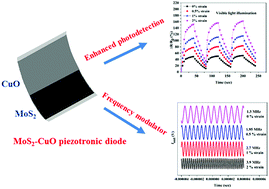
In this work, we demonstrate for the first time, a solution-processed MoS2 (n)–CuO (p) piezotronic diode on a flexible paper substrate for an enhanced broadband photodetector and active analog frequency modulator by application of external mechanical strain. There are no reports on solution-processed large area fabrication of MoS2-based heterojunctions wherein the external mechanical strain modulates the transport properties at the device level which can be further utilized at the circuit level for frequency modulation. When external strain is applied, because of the non-centrosymmetric structure of MoS2, the piezopotential induced adjusts the band structure at the junction and broadens the depletion region, which decreases the depletion capacitance of the diode. The widening of the depletion region improves the separation of photo-generated carriers and enhances the performance of the diode under both visible and NIR illumination. The fabricated piezotronic diode exhibited higher responsivity towards visible light illumination when compared to NIR illumination. The responsivity of the fabricated piezotronic diode increased by 69.7% under 2% strain. Such a versatile technique for fabrication of a diode and its utilization at both the device and circuit levels is a major step ahead in flexible and wearable electronics with applications ranging from digital, to analog, and optoelectronics.
中文翻译:

在纸基板上制造溶液处理的高度柔性的几层MoS 2(n)–CuO(p)压电二极管,用于有源模拟频率调制器和增强型宽带光电探测器
在这项工作中,我们首次展示了在柔性纸质基板上进行固溶处理的MoS 2(n)-CuO(p)压电二极管,通过施加外部机械应变来增强宽带光电探测器和有源模拟频率调制器。没有关于基于MoS 2的异质结的固溶处理大面积制造的报道,其中外部机械应变在器件级调节传输特性,该器件可以在电路级进一步用于频率调制。当施加外部应变时,由于MoS 2的非中心对称结构,所产生的压电势能调整结处的能带结构并加宽耗尽区,从而减小了二极管的耗尽电容。耗尽区的加宽改善了光生载流子的分离,并增强了可见光和近红外照明下二极管的性能。与NIR照明相比,所制造的压电二极管对可见光具有更高的响应度。在2%的应变下,制成的压电二极管的响应度提高了69.7%。这种用于二极管制造及其在器件和电路级的利用率的通用技术,在柔性和可穿戴电子设备中向前迈出了重要的一步,其应用范围从数字,模拟到光电。
更新日期:2017-11-16
中文翻译:
在纸基板上制造溶液处理的高度柔性的几层MoS 2(n)–CuO(p)压电二极管,用于有源模拟频率调制器和增强型宽带光电探测器
在这项工作中,我们首次展示了在柔性纸质基板上进行固溶处理的MoS 2(n)-CuO(p)压电二极管,通过施加外部机械应变来增强宽带光电探测器和有源模拟频率调制器。没有关于基于MoS 2的异质结的固溶处理大面积制造的报道,其中外部机械应变在器件级调节传输特性,该器件可以在电路级进一步用于频率调制。当施加外部应变时,由于MoS 2的非中心对称结构,所产生的压电势能调整结处的能带结构并加宽耗尽区,从而减小了二极管的耗尽电容。耗尽区的加宽改善了光生载流子的分离,并增强了可见光和近红外照明下二极管的性能。与NIR照明相比,所制造的压电二极管对可见光具有更高的响应度。在2%的应变下,制成的压电二极管的响应度提高了69.7%。这种用于二极管制造及其在器件和电路级的利用率的通用技术,在柔性和可穿戴电子设备中向前迈出了重要的一步,其应用范围从数字,模拟到光电。


 京公网安备 11010802027423号