当前位置:
X-MOL 学术
›
CrystEngComm
›
论文详情
Our official English website, www.x-mol.net, welcomes your
feedback! (Note: you will need to create a separate account there.)
Hierarchical architecture of CuInS2 microsphere thin films: altering laterally aligned crystallographic plane growth by Cd and V doping
CrystEngComm ( IF 2.6 ) Pub Date : 2017-10-02 00:00:00 , DOI: 10.1039/c7ce01293d Logu Thirumalaisamy 1, 2, 3, 4, 5 , Ramesh Raliya 1, 2, 3, 4, 5 , Shalinee Kavadiya 1, 2, 3, 4, 5 , Soundarrajan Palanivel 6, 7, 8, 9 , Kunjithapatham Sethuraman 6, 7, 8, 9 , Pratim Biswas 1, 2, 3, 4, 5
CrystEngComm ( IF 2.6 ) Pub Date : 2017-10-02 00:00:00 , DOI: 10.1039/c7ce01293d Logu Thirumalaisamy 1, 2, 3, 4, 5 , Ramesh Raliya 1, 2, 3, 4, 5 , Shalinee Kavadiya 1, 2, 3, 4, 5 , Soundarrajan Palanivel 6, 7, 8, 9 , Kunjithapatham Sethuraman 6, 7, 8, 9 , Pratim Biswas 1, 2, 3, 4, 5
Affiliation
|
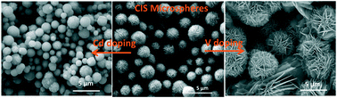
The hierarchical architecture of pristine and cadmium (Cd) and vanadium (V) doped copper indium disulphide (CuInS2 (CIS)) microsphere thin films grown on spray coated seed layers by a wet chemical method is demonstrated. First, nano-flakes of self-assembled porous (NFSAP)-CIS microspheres have been optimized on a CIS seed layer by controlling the synthesis strategy. Later, Cd and V were incorporated as foreign impurity ions into the NFSAP-CIS microspheres. The pristine and doped CIS microsphere films resulted in a body-centered-tetragonal crystal structure which was confirmed from the XRD and SAED patterns. The electron microscope images clearly depict the formation of a solid and an elongated NFSAP-CIS microsphere under Cd and V doping, respectively. The change in morphological structure was attributed to the suppression and expansion of the laterally oriented crystallographic plane. The chemical composition and optical and electrical properties of the pristine and Cd and V doped CIS films were determined by UV-vis, photoluminescence, XPS, and Hall measurements. The Cd and V doped CIS microsphere films have superior photoelectric response compared to the pristine CIS films. The controlled laterally oriented crystallographic plane in CIS microspheres brought about by doping induces the modification in the surface morphological structure that results in improved electrical and photo-physical properties. The results of this study provide a framework for fabricating an optimized CIS absorber layer in photovoltaic devices.
中文翻译:

CuInS 2微球薄膜的分层体系结构:通过Cd和V掺杂改变横向排列的晶体学平面生长
原始和镉(Cd)和钒(V)掺杂的铜铟二硫化物(CuInS 2(CIS))证明了通过湿化学方法在喷涂种子层上生长的微球薄膜。首先,通过控制合成策略,已在CIS种子层上优化了自组装多孔(NFSAP)-CIS微球的纳米薄片。后来,Cd和V作为外来杂质离子被掺入NFSAP-CIS微球中。原始和掺杂的CIS微球薄膜形成了以体心为中心的四边形晶体结构,这已通过XRD和SAED图案得到了证实。电子显微镜图像清楚地描绘了分别在Cd和V掺杂下形成固体和细长的NFSAP-CIS微球。形态结构的变化归因于横向取向晶体平面的抑制和扩展。原始的,Cd和V掺杂的CIS膜的化学成分以及光学和电学特性是通过UV-vis,光致发光,XPS和Hall测量来确定的。与原始CIS薄膜相比,Cd和V掺杂的CIS微球薄膜具有出色的光电响应。掺杂引起的CIS微球中可控的横向取向晶体学平面诱导了表面形态结构的修饰,从而改善了电学和光物理性质。这项研究的结果为在光伏器件中制造优化的CIS吸收层提供了框架。与原始CIS薄膜相比,Cd和V掺杂的CIS微球薄膜具有出色的光电响应。掺杂引起的CIS微球中可控的横向取向晶体学平面诱导了表面形态结构的修饰,从而改善了电学和光物理性质。这项研究的结果为在光伏器件中制造优化的CIS吸收层提供了框架。与原始CIS薄膜相比,Cd和V掺杂的CIS微球薄膜具有出色的光电响应。掺杂引起的CIS微球中可控的横向取向晶体学平面诱导了表面形态结构的修饰,从而改善了电学和光物理性质。这项研究的结果为在光伏器件中制造优化的CIS吸收层提供了框架。
更新日期:2017-11-13
中文翻译:
CuInS 2微球薄膜的分层体系结构:通过Cd和V掺杂改变横向排列的晶体学平面生长
原始和镉(Cd)和钒(V)掺杂的铜铟二硫化物(CuInS 2(CIS))证明了通过湿化学方法在喷涂种子层上生长的微球薄膜。首先,通过控制合成策略,已在CIS种子层上优化了自组装多孔(NFSAP)-CIS微球的纳米薄片。后来,Cd和V作为外来杂质离子被掺入NFSAP-CIS微球中。原始和掺杂的CIS微球薄膜形成了以体心为中心的四边形晶体结构,这已通过XRD和SAED图案得到了证实。电子显微镜图像清楚地描绘了分别在Cd和V掺杂下形成固体和细长的NFSAP-CIS微球。形态结构的变化归因于横向取向晶体平面的抑制和扩展。原始的,Cd和V掺杂的CIS膜的化学成分以及光学和电学特性是通过UV-vis,光致发光,XPS和Hall测量来确定的。与原始CIS薄膜相比,Cd和V掺杂的CIS微球薄膜具有出色的光电响应。掺杂引起的CIS微球中可控的横向取向晶体学平面诱导了表面形态结构的修饰,从而改善了电学和光物理性质。这项研究的结果为在光伏器件中制造优化的CIS吸收层提供了框架。与原始CIS薄膜相比,Cd和V掺杂的CIS微球薄膜具有出色的光电响应。掺杂引起的CIS微球中可控的横向取向晶体学平面诱导了表面形态结构的修饰,从而改善了电学和光物理性质。这项研究的结果为在光伏器件中制造优化的CIS吸收层提供了框架。与原始CIS薄膜相比,Cd和V掺杂的CIS微球薄膜具有出色的光电响应。掺杂引起的CIS微球中可控的横向取向晶体学平面诱导了表面形态结构的修饰,从而改善了电学和光物理性质。这项研究的结果为在光伏器件中制造优化的CIS吸收层提供了框架。


 京公网安备 11010802027423号