当前位置:
X-MOL 学术
›
Adv. Funct. Mater.
›
论文详情
Our official English website, www.x-mol.net, welcomes your feedback! (Note: you will need to create a separate account there.)
Mixed‐Dimensional 1D ZnO–2D WSe2 van der Waals Heterojunction Device for Photosensors
Advanced Functional Materials ( IF 19.0 ) Pub Date : 2017-11-02 , DOI: 10.1002/adfm.201703822 Young Tack Lee 1, 2 , Pyo Jin Jeon 3 , Jae Hyun Han 1, 4 , Jongtae Ahn 3 , Hyo Sun Lee 1 , June Yeong Lim 3 , Won Kook Choi 1, 5 , Jin Dong Song 1, 5 , Min-Chul Park 1, 5 , Seongil Im 3 , Do Kyung Hwang 1, 5
Advanced Functional Materials ( IF 19.0 ) Pub Date : 2017-11-02 , DOI: 10.1002/adfm.201703822 Young Tack Lee 1, 2 , Pyo Jin Jeon 3 , Jae Hyun Han 1, 4 , Jongtae Ahn 3 , Hyo Sun Lee 1 , June Yeong Lim 3 , Won Kook Choi 1, 5 , Jin Dong Song 1, 5 , Min-Chul Park 1, 5 , Seongil Im 3 , Do Kyung Hwang 1, 5
Affiliation
|
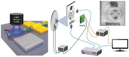
2D layered van der Waals (vdW) atomic crystals are an emerging class of new materials that are receiving increasing attention owing to their unique properties. In particular, the dangling‐bond‐free surface of 2D materials enables integration of differently dimensioned materials into mixed‐dimensional vdW heterostructures. Such mixed‐dimensional heterostructures herald new opportunities for conducting fundamental nanoscience studies and developing nanoscale electronic/optoelectronic applications. This study presents a 1D ZnO nanowire (n‐type)–2D WSe2 nanosheet (p‐type) vdW heterojunction diode for photodetection and imaging process. After amorphous fluoropolymer passivation, the ZnO–WSe2 diode shows superior performance with a much‐enhanced rectification (ON/OFF) ratio of over 106 and an ideality factor of 3.4–3.6 due to the carbon–fluorine (CF) dipole effect. This heterojunction device exhibits spectral photoresponses from ultraviolet (400 nm) to near infrared (950 nm). Furthermore, a prototype visible imager is demonstrated using the ZnO–WSe2 heterojunction diode as an imaging pixel. To the best of our knowledge, this is the first demonstration of an optoelectronic device based on a 1D–2D hybrid vdW heterojunction. This approach using a 1D ZnO–2D WSe2 heterojunction paves the way for the further development of electronic/optoelectronic applications using mixed‐dimensional vdW heterostructures.
中文翻译:

混合尺寸的一维ZnO–2D WSe2 van der Waals异质结器件,用于光电传感器
二维分层范德华(vdW)原子晶体是一类新兴的新材料,由于其独特的性能而受到越来越多的关注。特别是,二维材料的无悬空表面可以将尺寸不同的材料集成到混合尺寸的vdW异质结构中。这种混合的异质结构预示着进行基础纳米科学研究和开发纳米级电子/光电应用的新机会。这项研究提出了一种用于光电检测和成像过程的一维ZnO纳米线(n型)–2D WSe 2纳米片(p型)vdW异质结二极管。非晶态含氟聚合物钝化后,ZnO–WSe 2二极管表现出卓越的性能,整流(ON / OFF)比大大提高,超过10碳氟(C 3.4 F)偶极效应的影响,理想因数为6,理想因数为3.4-3.6 。这种异质结器件表现出从紫外(400 nm)到近红外(950 nm)的光谱光响应。此外,使用ZnO–WSe 2异质结二极管作为成像像素演示了可见光成像器原型。据我们所知,这是基于1D–2D混合vdW异质结的光电器件的首次演示。这种使用一维ZnO–2D WSe 2异质结的方法为使用混合vdW异质结构的电子/光电应用的进一步开发铺平了道路。
更新日期:2017-11-02
中文翻译:
混合尺寸的一维ZnO–2D WSe2 van der Waals异质结器件,用于光电传感器
二维分层范德华(vdW)原子晶体是一类新兴的新材料,由于其独特的性能而受到越来越多的关注。特别是,二维材料的无悬空表面可以将尺寸不同的材料集成到混合尺寸的vdW异质结构中。这种混合的异质结构预示着进行基础纳米科学研究和开发纳米级电子/光电应用的新机会。这项研究提出了一种用于光电检测和成像过程的一维ZnO纳米线(n型)–2D WSe 2纳米片(p型)vdW异质结二极管。非晶态含氟聚合物钝化后,ZnO–WSe 2二极管表现出卓越的性能,整流(ON / OFF)比大大提高,超过10碳氟(C 3.4 F)偶极效应的影响,理想因数为6,理想因数为3.4-3.6 。这种异质结器件表现出从紫外(400 nm)到近红外(950 nm)的光谱光响应。此外,使用ZnO–WSe 2异质结二极管作为成像像素演示了可见光成像器原型。据我们所知,这是基于1D–2D混合vdW异质结的光电器件的首次演示。这种使用一维ZnO–2D WSe 2异质结的方法为使用混合vdW异质结构的电子/光电应用的进一步开发铺平了道路。


 京公网安备 11010802027423号