当前位置:
X-MOL 学术
›
Adv. Electron. Mater.
›
论文详情
Our official English website, www.x-mol.net, welcomes your
feedback! (Note: you will need to create a separate account there.)
Fully Inkjet‐Printed Thin‐Film Transistor Array Manufactured on Paper Substrate for Cheap Electronic Applications
Advanced Electronic Materials ( IF 5.3 ) Pub Date : 2017-10-30 , DOI: 10.1002/aelm.201700275 Kalyan Yoti Mitra 1 , Maxim Polomoshnov 1 , Carme Martínez-Domingo 2, 3, 4 , Dana Mitra 1 , Eloi Ramon 3, 5 , Reinhard R. Baumann 1, 6
Advanced Electronic Materials ( IF 5.3 ) Pub Date : 2017-10-30 , DOI: 10.1002/aelm.201700275 Kalyan Yoti Mitra 1 , Maxim Polomoshnov 1 , Carme Martínez-Domingo 2, 3, 4 , Dana Mitra 1 , Eloi Ramon 3, 5 , Reinhard R. Baumann 1, 6
Affiliation
|
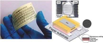
Over the past decade, inkjet technology has been well recognized for the manufacturing of products that include “printing beyond colors.” This micrometer‐scale precise technology provides a straightforward approach toward judicious deposition of electronically functional material inks on various substrates over relatively large areas, for printed/flexible electronics. The technology promotes upscalability and has become a renowned process tool for fabricating electronic devices in the field of printed/flexible electronics. Here, the fabrication of printed thin‐film transistors (TFT) on cheap coated paper substrate using inkjet technology is reported. For developing the TFT layer stack conductive nanoparticle inks, a polymeric dielectric ink and a p‐type organic semiconductor ink are employed. The coating on the paper provides several advantages for fabrication process of TFTs; for example, control over ink spreading. This control of ink spreading can directly influence the fabrication of interdigitated source/drain (S/D) electrodes for TFTs, when a top gate bottom contact architecture is considered. This results in better manufacturing yields and promising electrical performance, which are also the focus of this research. The all inkjet‐printed TFTs on paper exhibit electrical performance with maximum S/D current ranging to 170 nA, charge carrier mobility of 0.087 cm2 V−1 s−1, and current on/off ratio of 330.
中文翻译:

在纸基板上制造的全喷墨印刷薄膜晶体管阵列,可用于廉价的电子应用
在过去的十年中,喷墨技术在制造包括“超越色彩的印刷”的产品中得到了广泛认可。微米级的精密技术为明智地将电子功能材料油墨沉积在较大面积的各种基材上提供了一种简单的方法,适用于印刷/柔性电子产品。该技术提高了可扩展性,并已成为制造印刷/柔性电子领域中的电子设备的著名工艺工具。在这里,据报道使用喷墨技术在廉价的涂布纸基材上制造印刷薄膜晶体管(TFT)。为了开发TFT叠层导电纳米粒子油墨,使用了聚合物介电油墨和ap型有机半导体油墨。纸上的涂层为TFT的制造工艺提供了许多优势。例如,控制墨水扩散。当考虑顶栅底接触结构时,这种对油墨扩散的控制可以直接影响用于TFT的叉指式源/漏(S / D)电极的制造。这导致更好的制造良率和有希望的电性能,这也是本研究的重点。纸上所有喷墨打印的TFT均具有电气性能,最大S / D电流范围为170 nA,电荷载流子迁移率为0.087 cm 这导致更好的制造良率和有希望的电性能,这也是本研究的重点。纸上所有喷墨打印的TFT均具有电气性能,最大S / D电流达170 nA,载流子迁移率为0.087 cm 这导致更好的制造良率和有希望的电性能,这也是本研究的重点。纸上所有喷墨打印的TFT均具有电气性能,最大S / D电流范围为170 nA,电荷载流子迁移率为0.087 cm2 V -1 s -1,电流开/关比为330。
更新日期:2017-10-30
中文翻译:
在纸基板上制造的全喷墨印刷薄膜晶体管阵列,可用于廉价的电子应用
在过去的十年中,喷墨技术在制造包括“超越色彩的印刷”的产品中得到了广泛认可。微米级的精密技术为明智地将电子功能材料油墨沉积在较大面积的各种基材上提供了一种简单的方法,适用于印刷/柔性电子产品。该技术提高了可扩展性,并已成为制造印刷/柔性电子领域中的电子设备的著名工艺工具。在这里,据报道使用喷墨技术在廉价的涂布纸基材上制造印刷薄膜晶体管(TFT)。为了开发TFT叠层导电纳米粒子油墨,使用了聚合物介电油墨和ap型有机半导体油墨。纸上的涂层为TFT的制造工艺提供了许多优势。例如,控制墨水扩散。当考虑顶栅底接触结构时,这种对油墨扩散的控制可以直接影响用于TFT的叉指式源/漏(S / D)电极的制造。这导致更好的制造良率和有希望的电性能,这也是本研究的重点。纸上所有喷墨打印的TFT均具有电气性能,最大S / D电流范围为170 nA,电荷载流子迁移率为0.087 cm 这导致更好的制造良率和有希望的电性能,这也是本研究的重点。纸上所有喷墨打印的TFT均具有电气性能,最大S / D电流达170 nA,载流子迁移率为0.087 cm 这导致更好的制造良率和有希望的电性能,这也是本研究的重点。纸上所有喷墨打印的TFT均具有电气性能,最大S / D电流范围为170 nA,电荷载流子迁移率为0.087 cm2 V -1 s -1,电流开/关比为330。


 京公网安备 11010802027423号