当前位置:
X-MOL 学术
›
Adv. Electron. Mater.
›
论文详情
Our official English website, www.x-mol.net, welcomes your
feedback! (Note: you will need to create a separate account there.)
UV‐Sensing Semitransparent Organic Field‐Effect Transistors with Wide Bandgap Small Molecular Channel and Polymeric Gate‐Insulating Layers
Advanced Electronic Materials ( IF 5.3 ) Pub Date : 2017-09-18 , DOI: 10.1002/aelm.201700162 Chulyeon Lee 1 , Sooyong Lee 1 , Hwajeong Kim 1, 2 , Youngkyoo Kim 1
Advanced Electronic Materials ( IF 5.3 ) Pub Date : 2017-09-18 , DOI: 10.1002/aelm.201700162 Chulyeon Lee 1 , Sooyong Lee 1 , Hwajeong Kim 1, 2 , Youngkyoo Kim 1
Affiliation
|
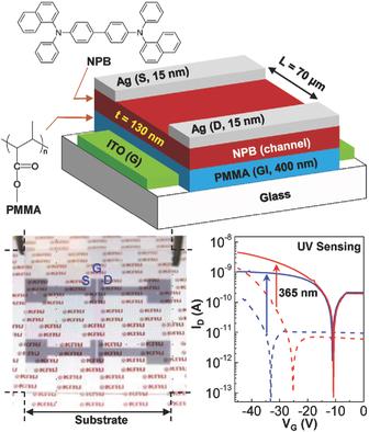
This study demonstrates UV‐sensing semitransparent organic field‐effect transistors (OFETs) with wide bandgap small molecular channel and polymeric gate‐insulating layers. N,N′‐di(1‐naphthyl)‐N,N′‐diphenyl‐(1,1′‐biphenyl)‐4,4′‐diamine (NPB) is employed as the wide bandgap channel layer, while poly(methyl methacrylate) is introduced as the wide bandgap gate‐insulating layer. The performance of OFETs is optimized by NPB thickness control and thermal treatment. Results show that the best device performance (on/off ratio = 4.7 × 10⁶ and hole mobility = 4.2 × 10⁻⁵ cm2 V−1 s−1) is achieved by thermal treatment of the 130 nm thick NPB layers at 70 °C for 30 min leading to a noticeably changed surface morphology in the NPB layers. The optimized OFETs exhibit excellent operation stability without hysteresis, while those with semitransparent silver electrodes deliver quite a good transparency. The semitransparent OFETs can sensitively detect a UV light with high stability even though no photoresponse is measured under a visible light.
中文翻译:

具有宽带隙小分子通道和聚合物栅绝缘层的UV感测半透明有机场效应晶体管
这项研究证明了具有宽带隙小分子通道和聚合物栅绝缘层的紫外线感应半透明有机场效应晶体管(OFET)。N,N'-二(1-萘基)-N,N'-二苯基-(1,1'-联苯)-4,4'-二胺(NPB)被用作宽带隙通道层,而聚(甲基甲基丙烯酸酯)被引入作为宽带隙栅绝缘层。通过NPB厚度控制和热处理优化了OFET的性能。结果表明,最佳器件性能(开/关比= 4.7×10 6,空穴迁移率= 4.2×10 -5 cm 2 V -1 s -1通过在70°C下对130 nm厚的NPB层进行30分钟的热处理可以实现Nb层表面形态的显着改变。经过优化的OFET具有出色的操作稳定性,而没有滞后现象,而带有半透明银电极的OFET具有非常好的透明度。即使在可见光下未测量到光响应,半透明的OFET仍可以灵敏地检测到具有高稳定性的紫外线。
更新日期:2017-09-18
中文翻译:
具有宽带隙小分子通道和聚合物栅绝缘层的UV感测半透明有机场效应晶体管
这项研究证明了具有宽带隙小分子通道和聚合物栅绝缘层的紫外线感应半透明有机场效应晶体管(OFET)。N,N'-二(1-萘基)-N,N'-二苯基-(1,1'-联苯)-4,4'-二胺(NPB)被用作宽带隙通道层,而聚(甲基甲基丙烯酸酯)被引入作为宽带隙栅绝缘层。通过NPB厚度控制和热处理优化了OFET的性能。结果表明,最佳器件性能(开/关比= 4.7×10 6,空穴迁移率= 4.2×10 -5 cm 2 V -1 s -1通过在70°C下对130 nm厚的NPB层进行30分钟的热处理可以实现Nb层表面形态的显着改变。经过优化的OFET具有出色的操作稳定性,而没有滞后现象,而带有半透明银电极的OFET具有非常好的透明度。即使在可见光下未测量到光响应,半透明的OFET仍可以灵敏地检测到具有高稳定性的紫外线。


 京公网安备 11010802027423号