当前位置:
X-MOL 学术
›
Adv. Electron. Mater.
›
论文详情
Our official English website, www.x-mol.net, welcomes your
feedback! (Note: you will need to create a separate account there.)
An Analytical Modeling of Field Electron Emission for a Vertical Wedged Ordered Nanostructure
Advanced Electronic Materials ( IF 5.3 ) Pub Date : 2017-08-16 , DOI: 10.1002/aelm.201700295 Yan Shen 1 , Ningsheng Xu 1 , Peng Ye 1 , Yu Zhang 1 , Fei Liu 1 , Jun Chen 1 , Juncong She 1 , Shaozhi Deng 1
Advanced Electronic Materials ( IF 5.3 ) Pub Date : 2017-08-16 , DOI: 10.1002/aelm.201700295 Yan Shen 1 , Ningsheng Xu 1 , Peng Ye 1 , Yu Zhang 1 , Fei Liu 1 , Jun Chen 1 , Juncong She 1 , Shaozhi Deng 1
Affiliation
|
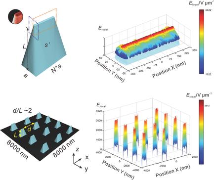
The development of field electron emission materials requires purposeful analytical modeling of structural features. A vertical wedged ordered nanostructure shows better field emission current density because of its in‐plane continuity at the top emission edge: Individually, its calculated average current density can be 8.3–26.7 times larger than a tapered nanostructure when its bottom area s increases from 0.5 to 2.5 µm2, can be 2.2–12.7 times as its radius of top curvature r decreases from 65 to 5 nm, and can be 7.3–17.3 times as its length L increases from 0.5 to 5 µm. For an ordered nanostructure array, its average current density can be about 160 times larger than the a reference tapered array when the individual elements are closely aligned. Over three orders of magnitude improvment can be observed when optimal emitter spacing conditions are used. Structural analytical models and numerical simulation prove to be in good correspondence with previously reported experimental data, and may serve as a guide for the design and preparation of field electron emission materials with a clear purpose in the future.
中文翻译:

垂直楔形有序纳米结构的场电子发射解析模型
场电子发射材料的发展需要对结构特征进行有目的的分析建模。垂直楔形有序纳米结构由于在顶部发射边缘具有面内连续性,因此具有更好的场发射电流密度:单独地,当其底部面积s从0.5增加时,其计算出的平均电流密度可以是锥形纳米结构的8.3–26.7倍。到2.5 µm 2,当其顶部曲率半径r从65减小到5 nm时可以是2.2–12.7倍,并且可以是其长度L的7.3–17.3倍从0.5微米增加到5微米。对于有序的纳米结构阵列,当各个元件紧密对齐时,其平均电流密度可以是参考锥形阵列的约160倍。当使用最佳发射极间隔条件时,可以观察到超过三个数量级的改进。结构分析模型和数值模拟证明与先前报道的实验数据高度吻合,并且可以作为未来明确目标的场电子发射材料的设计和制备的指南。
更新日期:2017-08-16
中文翻译:
垂直楔形有序纳米结构的场电子发射解析模型
场电子发射材料的发展需要对结构特征进行有目的的分析建模。垂直楔形有序纳米结构由于在顶部发射边缘具有面内连续性,因此具有更好的场发射电流密度:单独地,当其底部面积s从0.5增加时,其计算出的平均电流密度可以是锥形纳米结构的8.3–26.7倍。到2.5 µm 2,当其顶部曲率半径r从65减小到5 nm时可以是2.2–12.7倍,并且可以是其长度L的7.3–17.3倍从0.5微米增加到5微米。对于有序的纳米结构阵列,当各个元件紧密对齐时,其平均电流密度可以是参考锥形阵列的约160倍。当使用最佳发射极间隔条件时,可以观察到超过三个数量级的改进。结构分析模型和数值模拟证明与先前报道的实验数据高度吻合,并且可以作为未来明确目标的场电子发射材料的设计和制备的指南。


 京公网安备 11010802027423号