当前位置:
X-MOL 学术
›
Scr. Mater.
›
论文详情
Our official English website, www.x-mol.net, welcomes your feedback! (Note: you will need to create a separate account there.)
Van der Waals epitaxial AlGaN/GaN growth on hexagonal BN via two-dimensional N-induced dislocation slip
Scripta Materialia ( IF 6 ) Pub Date : 2024-04-27 , DOI: 10.1016/j.scriptamat.2024.116150 Ling Bai , Jing Ning , Haidi Wu , Boyu Wang , Dong Wang , Zhonghui Li , Yue Hao , Jincheng Zhang
Scripta Materialia ( IF 6 ) Pub Date : 2024-04-27 , DOI: 10.1016/j.scriptamat.2024.116150 Ling Bai , Jing Ning , Haidi Wu , Boyu Wang , Dong Wang , Zhonghui Li , Yue Hao , Jincheng Zhang
|
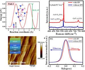
We demonstrate the epitaxial growth of nitride heterojunction structures on two-dimensional materials. The growth behavior of Al atoms on hexagonal boron nitride (h-BN) involves preferential adsorption and diffusion along the N-top position, considerably improving AlN formation in the early stage of nucleation. Preferential N adsorption enables h-BN to provide a natural N surface for the substrate. Moreover, the natural N surface provided by h-BN can induce three-dimensional island-like order merging of the upper AlN layer, promoting dislocation slip annihilation. The dislocations annihilation depth of GaN films was shortened to 870 nm, resulting in an order of magnitude decrease in the density of screw dislocations to 5.50 × 10 cm and considerable improvement in the performance of HEMT devices on SiC. Therefore, h-BN films can be used as two-dimensional insertion layers to obtain high-quality van der Waals epitaxial nitride films in GaN-based HEMT devices.
中文翻译:

通过二维 N 诱导位错滑移在六方 BN 上进行范德华外延 AlGaN/GaN 生长
我们展示了氮化物异质结结构在二维材料上的外延生长。 Al原子在六方氮化硼(h-BN)上的生长行为涉及沿N顶位置的优先吸附和扩散,显着改善了成核早期阶段的AlN形成。优先的 N 吸附使 h-BN 能够为基材提供天然的 N 表面。此外,h-BN提供的天然N表面可以诱导上AlN层的三维岛状有序合并,促进位错滑移湮灭。 GaN薄膜的位错湮灭深度缩短至870 nm,导致螺旋位错密度降低至5.50×10 cm,显着提高了SiC上HEMT器件的性能。因此,h-BN薄膜可以作为二维插入层,在GaN基HEMT器件中获得高质量的范德华外延氮化物薄膜。
更新日期:2024-04-27
中文翻译:
通过二维 N 诱导位错滑移在六方 BN 上进行范德华外延 AlGaN/GaN 生长
我们展示了氮化物异质结结构在二维材料上的外延生长。 Al原子在六方氮化硼(h-BN)上的生长行为涉及沿N顶位置的优先吸附和扩散,显着改善了成核早期阶段的AlN形成。优先的 N 吸附使 h-BN 能够为基材提供天然的 N 表面。此外,h-BN提供的天然N表面可以诱导上AlN层的三维岛状有序合并,促进位错滑移湮灭。 GaN薄膜的位错湮灭深度缩短至870 nm,导致螺旋位错密度降低至5.50×10 cm,显着提高了SiC上HEMT器件的性能。因此,h-BN薄膜可以作为二维插入层,在GaN基HEMT器件中获得高质量的范德华外延氮化物薄膜。


 京公网安备 11010802027423号