当前位置:
X-MOL 学术
›
Adv. Opt. Mater.
›
论文详情
Our official English website, www.x-mol.net, welcomes your feedback! (Note: you will need to create a separate account there.)
Structural, Optical, and Electronic Properties of Epitaxial β‐(AlxGa1‐x)2O3 Films for Optoelectronic Devices
Advanced Optical Materials ( IF 9 ) Pub Date : 2024-04-30 , DOI: 10.1002/adom.202400724 Fenhong Liu 1 , Yonghui Li 1 , Hongwei Cheng 1 , Chao Jin 1 , Changlong Liu 1
Advanced Optical Materials ( IF 9 ) Pub Date : 2024-04-30 , DOI: 10.1002/adom.202400724 Fenhong Liu 1 , Yonghui Li 1 , Hongwei Cheng 1 , Chao Jin 1 , Changlong Liu 1
Affiliation
|
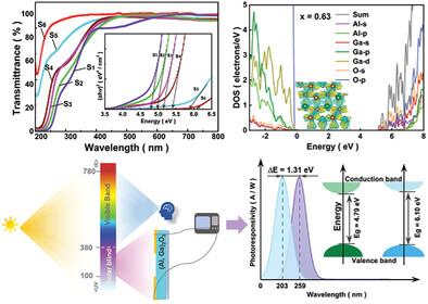
Bandgap engineering in monoclinic gallium oxide (β‐Ga2 O3 ) is a powerful strategy for designing semiconductor optoelectronic devices with specific functionalities. In this work, aluminum doping is utilized to modulate the bandgap of Ga2 O3 . By growing epitaxial β‐(Alx 1‐ x 2 O3 (0≤ x ≤ 0.84) films on c‐plane sapphire substrates using RF magnetron sputtering, it allowed to tune the energy bandgap, achieving values as high as 6.10 eV. The increased luminescence intensity is attributed to the recombination between donor and acceptor transitions induced by Al doping, resulting in more defects. Additionally, the luminescent band experienced blueshifts due to the enhanced bandgaps. Moreover, density of functional theory (DFT) simulations confirmed the sensitivity of the bandgap to Al content, distinguishing between Ga‐dominated (x < 0.5) and Al‐dominated (x > 0.5) β‐(Alx 1‐ x 2 O3 . Notably, the bandgap increased more rapidly in Ga‐dominated structures compared to Al‐dominated ones. The electronic structure analysis revealed a redistribution of Ga d states from valence to conduction bands, attributed to the introduction of numerous Al p states. These combined experimental and detailed electronic structure investigations proved crucial insights for designing the structure and exploring potential applications of β‐(Alx 1‐ x 2 O3 in photonic devices.
中文翻译:

用于光电器件的外延 β-(AlxGa1-x)2O3 薄膜的结构、光学和电子性能
单斜氧化镓(β-Ga2 氧3 )是设计具有特定功能的半导体光电器件的强大策略。在这项工作中,利用铝掺杂来调制Ga的带隙2 氧3 。通过外延生长 β-(AlX 1‐ X 2 氧3 (0≤X 使用射频磁控溅射在 c 面蓝宝石基板上制备 (≤ 0.84) 薄膜,可以调节能带隙,实现高达 6.10 eV 的值。发光强度的增加归因于Al掺杂引起的供体和受体跃迁之间的复合,导致更多的缺陷。此外,由于带隙增大,发光带经历了蓝移。此外,泛函密度理论 (DFT) 模拟证实了带隙对 Al 含量的敏感性,区分了 Ga 主导的 (X < 0.5) 和 Al 主导的 (X > 0.5) β-(铝X 1‐ X 2 氧3 。值得注意的是,与 Al 为主的结构相比,Ga 为主的结构的带隙增加得更快。电子结构分析揭示了Ga的重新分布d 从价态到导带的状态,归因于大量Al的引入p 状态。这些结合实验和详细的电子结构研究证明了设计结构和探索 β-(AlX 1‐ X 2 氧3 在光子器件中。
更新日期:2024-04-30
中文翻译:
用于光电器件的外延 β-(AlxGa1-x)2O3 薄膜的结构、光学和电子性能
单斜氧化镓(β-Ga


 京公网安备 11010802027423号