Our official English website, www.x-mol.net, welcomes your feedback! (Note: you will need to create a separate account there.)
Wafer Scale Gallium Nitride Integrated Electrode Toward Robust High Temperature Energy Storage
Small ( IF 13.3 ) Pub Date : 2024-04-21 , DOI: 10.1002/smll.202310837 Songyang Lv 1 , Shouzhi Wang 1, 2 , Jiaoxian Yu 3 , Ge Tian 4 , Guodong Wang 1 , Pengfei An 5 , Kepeng Song 1 , Bo Ma 5 , Yangyang Li 1 , Xiangang Xu 1 , Lei Zhang 1
Small ( IF 13.3 ) Pub Date : 2024-04-21 , DOI: 10.1002/smll.202310837 Songyang Lv 1 , Shouzhi Wang 1, 2 , Jiaoxian Yu 3 , Ge Tian 4 , Guodong Wang 1 , Pengfei An 5 , Kepeng Song 1 , Bo Ma 5 , Yangyang Li 1 , Xiangang Xu 1 , Lei Zhang 1
Affiliation
|
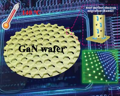
Gallium Nitride (GaN), as the representative of wide bandgap semiconductors, has great prospects in accomplishing rapid charge delivery under high-temperature environments thanks to excellent structural stability and electron mobility. However, there is still a gap in wafer-scale GaN single-crystal integrated electrodes applied in the energy storage field. Herein, Si-doped GaN nanochannel with gallium oxynitride (GaON) layer on a centimeter scale (denoted by GaN NC) is reported. The Si atoms modulate electronic redistribution to improve conductivity and drive nanochannel formation. Apart from that, the distinctive nanochannel configuration with a GaON layer provides adequate active sites and extraordinary structural stability. The GaN-based supercapacitors are assembled and deliver outstanding charge storage capabilities at 140 °C. Surprisingly, 90% retention is maintained after 50 000 cycles. This study opens the pathway toward wafer-scale GaN single-crystal integrated electrodes with self-powered characteristics that are compatible with various (opto)-electronic devices.
中文翻译:

晶圆级氮化镓集成电极实现稳健的高温储能
氮化镓(GaN)作为宽禁带半导体的代表,凭借优异的结构稳定性和电子迁移率,在高温环境下实现快速电荷传输具有广阔的前景。然而,晶圆级GaN单晶集成电极应用于储能领域仍存在差距。在此,报道了具有厘米级氮氧化镓(GaON)层的硅掺杂GaN纳米通道(用GaN NC表示)。 Si原子调节电子重新分布以提高电导率并驱动纳米通道的形成。除此之外,具有 GaON 层的独特纳米通道配置提供了足够的活性位点和非凡的结构稳定性。 GaN 基超级电容器在 140°C 下组装并提供出色的电荷存储能力。令人惊讶的是,50000 次循环后仍保持 90% 的保留率。这项研究为晶圆级 GaN 单晶集成电极开辟了道路,该电极具有与各种(光电)电子设备兼容的自供电特性。
更新日期:2024-04-21
中文翻译:
晶圆级氮化镓集成电极实现稳健的高温储能
氮化镓(GaN)作为宽禁带半导体的代表,凭借优异的结构稳定性和电子迁移率,在高温环境下实现快速电荷传输具有广阔的前景。然而,晶圆级GaN单晶集成电极应用于储能领域仍存在差距。在此,报道了具有厘米级氮氧化镓(GaON)层的硅掺杂GaN纳米通道(用GaN NC表示)。 Si原子调节电子重新分布以提高电导率并驱动纳米通道的形成。除此之外,具有 GaON 层的独特纳米通道配置提供了足够的活性位点和非凡的结构稳定性。 GaN 基超级电容器在 140°C 下组装并提供出色的电荷存储能力。令人惊讶的是,50000 次循环后仍保持 90% 的保留率。这项研究为晶圆级 GaN 单晶集成电极开辟了道路,该电极具有与各种(光电)电子设备兼容的自供电特性。


 京公网安备 11010802027423号