当前位置:
X-MOL 学术
›
Appl. Surf. Sci.
›
论文详情
Our official English website, www.x-mol.net, welcomes your feedback! (Note: you will need to create a separate account there.)
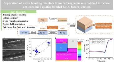
Separation of wafer bonding interface from heterogenous mismatched interface achieved high quality bonded Ge-Si heterojunction
Applied Surface Science ( IF 6.7 ) Pub Date : 2024-04-15 , DOI: 10.1016/j.apsusc.2024.160104 Ruoyun Ji , Dan Wang , Jinlong Jiao , Liqiang Yao , Fuxiu He , Cheng Li , Guangyang Lin , Fuming Wang , Wei Huang , Songyan Chen
Applied Surface Science ( IF 6.7 ) Pub Date : 2024-04-15 , DOI: 10.1016/j.apsusc.2024.160104 Ruoyun Ji , Dan Wang , Jinlong Jiao , Liqiang Yao , Fuxiu He , Cheng Li , Guangyang Lin , Fuming Wang , Wei Huang , Songyan Chen
|
In the realm of optoelectronic integration, silicon-based Ge bonding has attracted great attention due to its advantages in short-wave infrared response and low cost. However, owing to the inherent lattice mismatch and thermal mismatch between Ge and Si, the bonded Ge-Si heterogenous interfaces encountered problems of thermal instability and high interface states. Herein, an approach of separating the bonding interface from the heterogenous interface is proposed through inserting a Ge epitaxial layer (GeEL) between the Si substrate and Ge film. This separation modifies the bonding interface to a homogenous one, alleviating the massive mismatch stress and achieving film relaxation, enhancing bonding stability in all aspects. Moreover, during 850 °C annealing, GeEL is doped via diffusion hence realizes electric filed modulation, inhibiting the carrier recombination leakage current and trap assisted tunneling in this defect-rich layer. A Ge-Si heterogenous PIN diode prepared by this bonding method has achieved a remarkable low dark current density (1.33 mA/cm), a low ideality factor (1.11), and a high on–off ratio (10), confirming the outstanding quality of the bonded heterojunction. This work provides great prospects for higher performance, larger scale and multi-functional Si-based heterogenous material device applications.
中文翻译:

将晶圆键合界面与异质失配界面分离,实现高质量键合Ge-Si异质结
在光电集成领域,硅基Ge键合因其短波红外响应和低成本的优势而受到广泛关注。然而,由于Ge和Si之间固有的晶格失配和热失配,键合的Ge-Si异质界面遇到了热不稳定和高界面态的问题。本文提出了一种通过在Si衬底和Ge薄膜之间插入Ge外延层(GeEL)来将键合界面与异质界面分离的方法。这种分离使键合界面变得均匀,减轻了巨大的失配应力并实现了薄膜松弛,从而增强了各方面的键合稳定性。此外,在850℃退火过程中,GeEL通过扩散进行掺杂,从而实现电场调制,抑制了该缺陷丰富层中的载流子复合漏电流和陷阱辅助隧道效应。通过这种键合方法制备的Ge-Si异质PIN二极管实现了显着的低暗电流密度(1.33 mA/cm)、低理想因子(1.11)和高开关比(10),证实了卓越的质量键合异质结。该工作为更高性能、更大规模、多功能的硅基异质材料器件应用提供了广阔的前景。
更新日期:2024-04-15
中文翻译:
将晶圆键合界面与异质失配界面分离,实现高质量键合Ge-Si异质结
在光电集成领域,硅基Ge键合因其短波红外响应和低成本的优势而受到广泛关注。然而,由于Ge和Si之间固有的晶格失配和热失配,键合的Ge-Si异质界面遇到了热不稳定和高界面态的问题。本文提出了一种通过在Si衬底和Ge薄膜之间插入Ge外延层(GeEL)来将键合界面与异质界面分离的方法。这种分离使键合界面变得均匀,减轻了巨大的失配应力并实现了薄膜松弛,从而增强了各方面的键合稳定性。此外,在850℃退火过程中,GeEL通过扩散进行掺杂,从而实现电场调制,抑制了该缺陷丰富层中的载流子复合漏电流和陷阱辅助隧道效应。通过这种键合方法制备的Ge-Si异质PIN二极管实现了显着的低暗电流密度(1.33 mA/cm)、低理想因子(1.11)和高开关比(10),证实了卓越的质量键合异质结。该工作为更高性能、更大规模、多功能的硅基异质材料器件应用提供了广阔的前景。


 京公网安备 11010802027423号