当前位置:
X-MOL 学术
›
Laser Photonics Rev.
›
论文详情
Our official English website, www.x-mol.net, welcomes your feedback! (Note: you will need to create a separate account there.)
Silicon Nanoantennas for Ultra‐Compact, High‐Speed and Low‐Power Consumption Electro‐Optic Modulators
Laser & Photonics Reviews ( IF 11.0 ) Pub Date : 2024-04-12 , DOI: 10.1002/lpor.202301068 Lu Ding 1 , Shawn Yohanes Siew 2 , Thomas Y. L. Ang 3 , Qiang Li 2 , Shiyang Zhu 4 , Yanyan Zhou 4 , Ramon Paniagua‐Dominguez 1 , Hong‐Son Chu 3 , Soon Thor Lim 3 , Ching Eng Png 3 , Arseniy I. Kuznetsov 1
Laser & Photonics Reviews ( IF 11.0 ) Pub Date : 2024-04-12 , DOI: 10.1002/lpor.202301068 Lu Ding 1 , Shawn Yohanes Siew 2 , Thomas Y. L. Ang 3 , Qiang Li 2 , Shiyang Zhu 4 , Yanyan Zhou 4 , Ramon Paniagua‐Dominguez 1 , Hong‐Son Chu 3 , Soon Thor Lim 3 , Ching Eng Png 3 , Arseniy I. Kuznetsov 1
Affiliation
|
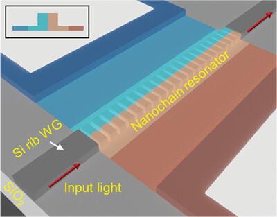
To keep pace with the expanding data capacity in modern communications and increasing on‐chip integration density, it is highly desirable to have electro‐optic modulators featured with compact footprint, large modulation bandwidth, low energy consumption, and full complementary metal‐oxide‐semiconductor (CMOS) compatibility. Here, this work experimentally demonstrates a high‐speed electro‐optic modulator in the telecommunication wavelength range made of a 1D chain resonator of Mie‐resonant silicon nanoparticles. The modulator exploits the plasma dispersion effect and works in the carrier depletion configuration. The resulting large modulation bandwidth over 40 GHz and low energy consumption of 23 fJ bit−1 are attributed to its ultra‐compact footprint of 10 µm2 . The open eye diagrams are measured up to 40 Gbits s−1 . The modulators are fabricated at wafer level by a silicon photonic foundry using CMOS‐compatible process. This modulator shows promise for achieving higher integration density and larger modulation bandwidth. It can be added to the existing on‐chip device building blocks library and used for a wide range of applications, including data communication, quantum photonics, and non‐reciprocal optics.
中文翻译:

用于超紧凑、高速和低功耗电光调制器的硅纳米天线
为了跟上现代通信中不断增长的数据容量和不断增加的片上集成密度,非常需要具有紧凑占地面积、大调制带宽、低能耗和全互补金属氧化物半导体的电光调制器(CMOS)兼容性。在这里,这项工作通过实验展示了一种由米氏共振硅纳米颗粒的一维链谐振器制成的电信波长范围内的高速电光调制器。该调制器利用等离子体色散效应并在载流子耗尽配置中工作。由此产生超过 40 GHz 的大调制带宽和 23 fJ 位的低能耗−1 归因于其 10 µm 的超紧凑占地面积2 。开眼图测量速率高达 40 Gbits−1 。调制器由硅光子铸造厂采用 CMOS 兼容工艺在晶圆级制造。该调制器有望实现更高的集成密度和更大的调制带宽。它可以添加到现有的片上设备构建模块库中,并用于广泛的应用,包括数据通信、量子光子学和非互易光学。
更新日期:2024-04-12
中文翻译:
用于超紧凑、高速和低功耗电光调制器的硅纳米天线
为了跟上现代通信中不断增长的数据容量和不断增加的片上集成密度,非常需要具有紧凑占地面积、大调制带宽、低能耗和全互补金属氧化物半导体的电光调制器(CMOS)兼容性。在这里,这项工作通过实验展示了一种由米氏共振硅纳米颗粒的一维链谐振器制成的电信波长范围内的高速电光调制器。该调制器利用等离子体色散效应并在载流子耗尽配置中工作。由此产生超过 40 GHz 的大调制带宽和 23 fJ 位的低能耗


 京公网安备 11010802027423号