Our official English website, www.x-mol.net, welcomes your feedback! (Note: you will need to create a separate account there.)
Wide‐Gap Perovskites for Indoor Photovoltaics
Solar RRL ( IF 7.9 ) Pub Date : 2024-04-12 , DOI: 10.1002/solr.202400180 Gregory Burwell 1 , Stefan Zeiske 1, 2 , Pietro Caprioglio 3 , Oskar J. Sandberg 1, 4 , Austin M. Kay 1 , Michael D. Farrar 3 , Yong Ryun Kim 1, 5 , Henry J. Snaith 3 , Paul Meredith 1 , Ardalan Armin 1
Solar RRL ( IF 7.9 ) Pub Date : 2024-04-12 , DOI: 10.1002/solr.202400180 Gregory Burwell 1 , Stefan Zeiske 1, 2 , Pietro Caprioglio 3 , Oskar J. Sandberg 1, 4 , Austin M. Kay 1 , Michael D. Farrar 3 , Yong Ryun Kim 1, 5 , Henry J. Snaith 3 , Paul Meredith 1 , Ardalan Armin 1
Affiliation
|
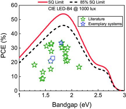
Organic–inorganic halide perovskite semiconductors have revolutionized next‐generation photovoltaics (PV) due to several characteristics such as solution‐processability, gap tunability, and excellent charge generation and transport properties. This has made them very adaptable for various applications in light harvesting and photodetection. One such rapidly growing application is indoor photovoltaics (IPV) which have the potential to power standalone Internet of Things devices. IPV requires wider optimal bandgaps than solar cells (1.8 vs 1.3 eV) due to the differences between the spectra of artificial lights versus solar radiation. For IPV applications, the active layer wide‐gap perovskite must be developed systemically considering all other components of the device, such as interlayers, electrodes, and scaling. This perspective provides an overview of the potential and challenges facing perovskite‐based IPV from a theoretical, material, and experimental perspective. Furthermore, accurate characterization of perovskite IPVs under simulated indoor conditions is discussed and candidate perovskite PV (PPV) systems are presented to provide insight into IPV development. These include IPV‐optimized formamidinium cesium‐based perovskite, wide‐gap p‐i‐n devices, and 2D perovskite devices, tested under spectrophotometrically calibrated LED illumination at various indoor‐relevant illuminances and benchmarked against thermodynamic predictions. Finally, strategies required to create stable, optimized PPV devices for indoor applications are discussed.
中文翻译:

用于室内光伏的宽禁带钙钛矿
有机-无机卤化物钙钛矿半导体由于具有溶液加工性、间隙可调性以及优异的电荷产生和传输性能等多种特性,已经彻底改变了下一代光伏(PV)。这使得它们非常适合光采集和光电检测中的各种应用。其中一种快速增长的应用是室内光伏 (IPV),它有潜力为独立的物联网设备供电。由于人造光与太阳辐射光谱之间的差异,IPV 需要比太阳能电池更宽的最佳带隙(1.8 与 1.3 eV)。对于 IPV 应用,有源层宽禁带钙钛矿的开发必须系统地考虑设备的所有其他组件,例如中间层、电极和缩放。该观点从理论、材料和实验的角度概述了基于钙钛矿的 IPV 所面临的潜力和挑战。此外,还讨论了模拟室内条件下钙钛矿 IPV 的准确表征,并提出了候选钙钛矿光伏 (PPV) 系统,以深入了解 IPV 的开发。其中包括 IPV 优化的甲脒铯基钙钛矿、宽禁带 p-i-n 器件和 2D 钙钛矿器件,在各种室内相关照度下的分光光度校准 LED 照明下进行测试,并根据热力学预测进行基准测试。最后,讨论了为室内应用创建稳定、优化的 PPV 设备所需的策略。
更新日期:2024-04-12
中文翻译:
用于室内光伏的宽禁带钙钛矿
有机-无机卤化物钙钛矿半导体由于具有溶液加工性、间隙可调性以及优异的电荷产生和传输性能等多种特性,已经彻底改变了下一代光伏(PV)。这使得它们非常适合光采集和光电检测中的各种应用。其中一种快速增长的应用是室内光伏 (IPV),它有潜力为独立的物联网设备供电。由于人造光与太阳辐射光谱之间的差异,IPV 需要比太阳能电池更宽的最佳带隙(1.8 与 1.3 eV)。对于 IPV 应用,有源层宽禁带钙钛矿的开发必须系统地考虑设备的所有其他组件,例如中间层、电极和缩放。该观点从理论、材料和实验的角度概述了基于钙钛矿的 IPV 所面临的潜力和挑战。此外,还讨论了模拟室内条件下钙钛矿 IPV 的准确表征,并提出了候选钙钛矿光伏 (PPV) 系统,以深入了解 IPV 的开发。其中包括 IPV 优化的甲脒铯基钙钛矿、宽禁带 p-i-n 器件和 2D 钙钛矿器件,在各种室内相关照度下的分光光度校准 LED 照明下进行测试,并根据热力学预测进行基准测试。最后,讨论了为室内应用创建稳定、优化的 PPV 设备所需的策略。


 京公网安备 11010802027423号