当前位置:
X-MOL 学术
›
ACS Energy Lett.
›
论文详情
Our official English website, www.x-mol.net, welcomes your feedback! (Note: you will need to create a separate account there.)
Recent Progress in Regulating Surface Potential for High-Efficiency Perovskite Solar Cells
ACS Energy Letters ( IF 22.0 ) Pub Date : 2024-03-22 , DOI: 10.1021/acsenergylett.4c00240 Jiaheng Nie 1 , Yaming Zhang 2 , Jizheng Wang 3 , Lijie Li 4 , Yan Zhang 2
ACS Energy Letters ( IF 22.0 ) Pub Date : 2024-03-22 , DOI: 10.1021/acsenergylett.4c00240 Jiaheng Nie 1 , Yaming Zhang 2 , Jizheng Wang 3 , Lijie Li 4 , Yan Zhang 2
Affiliation
|
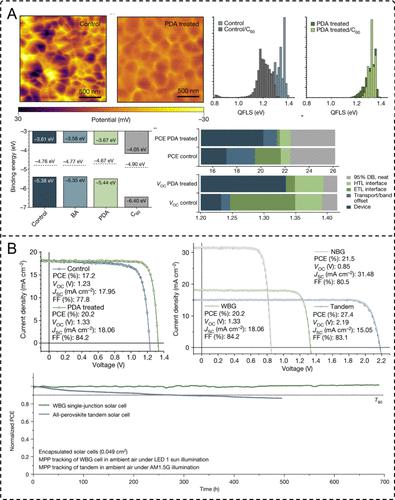
Figure 1. (a) KPFM images, histograms of QFLS, band alignment for control and PDA-treated films, and loss analysis for PCE and VOC of devices with control and PDA treatment. Reproduced with permission from ref (7). Copyright 2022 Springer Nature. (b) J–V curves of NBG, WBG, and all-perovskite tandem devices, and stability measurement of WBG and all-perovskite tandem devices. Reproduced with permission from ref (7). Copyright 2022 Springer Nature. Figure 2. (a) KPFM data and J–V measurement of control and target device. Reproduced with permission from ref (3). Copyright 2022 Springer Nature. (b) Surface potential images measured by KPFM, J–V curves, and histograms of the PCE data with and without FcTc2. Reproduced with permission from ref (4). Copyright 2022 American Association for the Advancement of Science. (c) J–V curves of device and energy-level alignment of different interface. Reproduced with permission from ref (5). Copyright 2023 American Association for the Advancement of Science. Figure 3. (a) KPFM images of films with and without F4TCNQ, schematic of the energy diagram of interface between perovskite and F4TCNQ layer. Reprinted or adapted with permission from ref (14). Copyright 2018 Springer Nature, CC-BY 4.0 (https://creativecommons.org/licenses/by/4.0/). (b) Schematic of interfacial hole transfer dynamics. Reprinted or adapted with permission from ref (14). Copyright 2018 Springer Nature, CC-BY 4.0 (https://creativecommons.org/licenses/by/4.0/). Figure 4. (a) Surface potential maps and work function distributions of reference, OAI-treated, and OATsO-treated devices. Reproduced with permission from ref (6). Copyright 2022 Springer Nature. (b) Electric field distribution, charge density distribution, and band diagrams of OAI-treated and OATsO-treated devices. Reproduced with permission from ref (6). Copyright 2022 Springer Nature. (c) PCE and stability measurement of OAI-treated and OATsO-treated devices. Reproduced with permission from ref (6). Copyright 2022 Springer Nature. Further investigation of the influence of uniform surface potential distribution of perovskites on interfacial barriers is needed. How surface potential uniformity reduces interfacial recombination and enhances carrier injection must be determined. The relationship between external electric field or polarization and junction/interface requires additional attention. Schottky barrier height should be investigated through cross-sectional surface potential distribution characterized by KPFM. Experiments have shown that chemical methods such as doping and adding interlayers can effectively tune the surface potential distribution or interfacial charge transfer. It remains to be explored whether electric field modulation is a viable and effective approach to regulate interfacial barriers and enhance device performance. Polarization induced by external electric fields can promote device performance through precise control of barriers, thereby contributing to future low-cost scalable manufacturing; this needs to be explored. The authors are thankful for support from Major Program of National Natural Science Foundation of China (Grant Nos. 52192610, 52192612) and Key Program of National Natural Science Foundation of China (Grant No. U22A2077). The authors are thankful for the support by the Fundamental Research Funds for the Central Universities (Grant No. ZYGX2021YGCX001). This article references 17 other publications. This article has not yet been cited by other publications. Figure 1. (a) KPFM images, histograms of QFLS, band alignment for control and PDA-treated films, and loss analysis for PCE and VOC of devices with control and PDA treatment. Reproduced with permission from ref (7). Copyright 2022 Springer Nature. (b) J–V curves of NBG, WBG, and all-perovskite tandem devices, and stability measurement of WBG and all-perovskite tandem devices. Reproduced with permission from ref (7). Copyright 2022 Springer Nature. Figure 2. (a) KPFM data and J–V measurement of control and target device. Reproduced with permission from ref (3). Copyright 2022 Springer Nature. (b) Surface potential images measured by KPFM, J–V curves, and histograms of the PCE data with and without FcTc2. Reproduced with permission from ref (4). Copyright 2022 American Association for the Advancement of Science. (c) J–V curves of device and energy-level alignment of different interface. Reproduced with permission from ref (5). Copyright 2023 American Association for the Advancement of Science. Figure 3. (a) KPFM images of films with and without F4TCNQ, schematic of the energy diagram of interface between perovskite and F4TCNQ layer. Reprinted or adapted with permission from ref (14). Copyright 2018 Springer Nature, CC-BY 4.0 (https://creativecommons.org/licenses/by/4.0/). (b) Schematic of interfacial hole transfer dynamics. Reprinted or adapted with permission from ref (14). Copyright 2018 Springer Nature, CC-BY 4.0 (https://creativecommons.org/licenses/by/4.0/). Figure 4. (a) Surface potential maps and work function distributions of reference, OAI-treated, and OATsO-treated devices. Reproduced with permission from ref (6). Copyright 2022 Springer Nature. (b) Electric field distribution, charge density distribution, and band diagrams of OAI-treated and OATsO-treated devices. Reproduced with permission from ref (6). Copyright 2022 Springer Nature. (c) PCE and stability measurement of OAI-treated and OATsO-treated devices. Reproduced with permission from ref (6). Copyright 2022 Springer Nature. This article references 17 other publications.
中文翻译:

调节高效钙钛矿太阳能电池表面电位的最新进展
图 1. (a) KPFM 图像、QFLS 直方图、对照和 PDA 处理薄膜的条带排列,以及经过对照和 PDA 处理的器件的PCE 和VOC损失分析。经参考文献 (7) 许可转载。版权所有 2022 施普林格自然。 (b) NBG、WBG和全钙钛矿串联器件的J - V曲线,以及WBG和全钙钛矿串联器件的稳定性测量。经参考文献 (7) 许可转载。版权所有 2022 施普林格自然。图 2.(a)控制和目标设备的KPFM 数据和J – V测量。经参考文献 (3) 许可转载。版权所有 2022 施普林格自然。 (b) 通过 KPFM 测量的表面电位图像、J – V曲线以及有和没有 FcTc 2的 PCE 数据的直方图。经参考文献 (4) 许可转载。版权所有 2022 美国科学促进会。 (c) J – V器件曲线和不同界面的能级排列。经参考文献 (5) 许可转载。版权所有 2023 美国科学促进会。图 3. (a) 有和没有 F4TCNQ 的薄膜的 KPFM 图像,钙钛矿和 F4TCNQ 层之间界面的能量图示意图。经参考文献 (14) 许可重印或改编。版权所有 2018 施普林格自然,CC-BY 4.0 (https://creativecommons.org/licenses/by/4.0/)。 (b) 界面空穴传输动力学示意图。经参考文献 (14) 许可重印或改编。版权所有 2018 施普林格自然,CC-BY 4.0 (https://creativecommons.org/licenses/by/4.0/)。图 4.(a) 参考器件、OAI 处理器件和 OATsO 处理器件的表面电势图和功函数分布。经参考文献 (6) 许可转载。版权所有 2022 施普林格自然。 (b) OAI 处理和 OATsO 处理器件的电场分布、电荷密度分布和能带图。经参考文献 (6) 许可转载。版权所有 2022 施普林格自然。 (c) OAI 处理和 OATsO 处理设备的 PCE 和稳定性测量。经参考文献 (6) 许可转载。版权所有 2022 施普林格自然。需要进一步研究钙钛矿均匀表面电位分布对界面势垒的影响。必须确定表面电势均匀性如何减少界面复合并增强载流子注入。外部电场或极化与结/界面之间的关系需要额外注意。肖特基势垒高度应通过 KPFM 表征的横截面表面电势分布来研究。实验表明,掺杂和添加中间层等化学方法可以有效地调节表面电位分布或界面电荷转移。电场调制是否是调节界面势垒和增强器件性能的可行且有效的方法仍有待探索。外部电场引起的极化可以通过精确控制势垒来提升器件性能,从而有助于未来的低成本可扩展制造;这需要探索。作者感谢国家自然科学基金重大项目(批准号:52192610、52192612)和国家自然科学基金重点项目(批准号:U22A2077)的支持。作者感谢中央高校基本科研业务费专项资金(批准号:ZYGX2021YGCX001)的支持。本文引用了其他 17 篇出版物。这篇文章尚未被其他出版物引用。图 1. (a) KPFM 图像、QFLS 直方图、对照膜和 PDA 处理膜的谱带排列,以及对照膜和 PDA 处理设备的PCE 和V OC损失分析。经参考文献 (7) 许可转载。版权所有 2022 施普林格自然。 (二)NBG、WBG和全钙钛矿串联器件的J - V曲线,以及WBG和全钙钛矿串联器件的稳定性测量。经参考文献 (7) 许可转载。版权所有 2022 施普林格自然。图 2.(a)控制和目标设备的KPFM 数据和J – V测量。经参考文献 (3) 许可转载。版权所有 2022 施普林格自然。 (b) 通过 KPFM 测量的表面电位图像、J – V曲线以及有和没有 FcTc 2的 PCE 数据的直方图。经参考文献 (4) 许可转载。版权所有 2022 美国科学促进会。 (c)器件的J - V曲线和不同界面的能级排列。经参考文献 (5) 许可转载。版权所有 2023 美国科学促进会。图 3. (a) 有和没有 F4TCNQ 的薄膜的 KPFM 图像,钙钛矿和 F4TCNQ 层之间界面的能量图示意图。经参考文献 (14) 许可重印或改编。版权所有 2018 施普林格自然,CC-BY 4.0 (https://creativecommons.org/licenses/by/4.0/)。 (b) 界面空穴传输动力学示意图。经参考文献 (14) 许可重印或改编。版权所有 2018 施普林格自然,CC-BY 4.0 (https://creativecommons.org/licenses/by/4.0/)。图 4.(a) 参考器件、OAI 处理器件和 OATsO 处理器件的表面电势图和功函数分布。经参考文献 (6) 许可转载。版权所有 2022 施普林格自然。 (b) OAI 处理和 OATsO 处理器件的电场分布、电荷密度分布和能带图。经参考文献 (6) 许可转载。版权所有 2022 施普林格自然。 (c) OAI 处理和 OATsO 处理设备的 PCE 和稳定性测量。经参考文献 (6) 许可转载。版权所有 2022 施普林格自然。本文引用了其他 17 篇出版物。
更新日期:2024-03-22
中文翻译:
调节高效钙钛矿太阳能电池表面电位的最新进展
图 1. (a) KPFM 图像、QFLS 直方图、对照和 PDA 处理薄膜的条带排列,以及经过对照和 PDA 处理的器件的PCE 和VOC损失分析。经参考文献 (7) 许可转载。版权所有 2022 施普林格自然。 (b) NBG、WBG和全钙钛矿串联器件的J - V曲线,以及WBG和全钙钛矿串联器件的稳定性测量。经参考文献 (7) 许可转载。版权所有 2022 施普林格自然。图 2.(a)控制和目标设备的KPFM 数据和J – V测量。经参考文献 (3) 许可转载。版权所有 2022 施普林格自然。 (b) 通过 KPFM 测量的表面电位图像、J – V曲线以及有和没有 FcTc 2的 PCE 数据的直方图。经参考文献 (4) 许可转载。版权所有 2022 美国科学促进会。 (c) J – V器件曲线和不同界面的能级排列。经参考文献 (5) 许可转载。版权所有 2023 美国科学促进会。图 3. (a) 有和没有 F4TCNQ 的薄膜的 KPFM 图像,钙钛矿和 F4TCNQ 层之间界面的能量图示意图。经参考文献 (14) 许可重印或改编。版权所有 2018 施普林格自然,CC-BY 4.0 (https://creativecommons.org/licenses/by/4.0/)。 (b) 界面空穴传输动力学示意图。经参考文献 (14) 许可重印或改编。版权所有 2018 施普林格自然,CC-BY 4.0 (https://creativecommons.org/licenses/by/4.0/)。图 4.(a) 参考器件、OAI 处理器件和 OATsO 处理器件的表面电势图和功函数分布。经参考文献 (6) 许可转载。版权所有 2022 施普林格自然。 (b) OAI 处理和 OATsO 处理器件的电场分布、电荷密度分布和能带图。经参考文献 (6) 许可转载。版权所有 2022 施普林格自然。 (c) OAI 处理和 OATsO 处理设备的 PCE 和稳定性测量。经参考文献 (6) 许可转载。版权所有 2022 施普林格自然。需要进一步研究钙钛矿均匀表面电位分布对界面势垒的影响。必须确定表面电势均匀性如何减少界面复合并增强载流子注入。外部电场或极化与结/界面之间的关系需要额外注意。肖特基势垒高度应通过 KPFM 表征的横截面表面电势分布来研究。实验表明,掺杂和添加中间层等化学方法可以有效地调节表面电位分布或界面电荷转移。电场调制是否是调节界面势垒和增强器件性能的可行且有效的方法仍有待探索。外部电场引起的极化可以通过精确控制势垒来提升器件性能,从而有助于未来的低成本可扩展制造;这需要探索。作者感谢国家自然科学基金重大项目(批准号:52192610、52192612)和国家自然科学基金重点项目(批准号:U22A2077)的支持。作者感谢中央高校基本科研业务费专项资金(批准号:ZYGX2021YGCX001)的支持。本文引用了其他 17 篇出版物。这篇文章尚未被其他出版物引用。图 1. (a) KPFM 图像、QFLS 直方图、对照膜和 PDA 处理膜的谱带排列,以及对照膜和 PDA 处理设备的PCE 和V OC损失分析。经参考文献 (7) 许可转载。版权所有 2022 施普林格自然。 (二)NBG、WBG和全钙钛矿串联器件的J - V曲线,以及WBG和全钙钛矿串联器件的稳定性测量。经参考文献 (7) 许可转载。版权所有 2022 施普林格自然。图 2.(a)控制和目标设备的KPFM 数据和J – V测量。经参考文献 (3) 许可转载。版权所有 2022 施普林格自然。 (b) 通过 KPFM 测量的表面电位图像、J – V曲线以及有和没有 FcTc 2的 PCE 数据的直方图。经参考文献 (4) 许可转载。版权所有 2022 美国科学促进会。 (c)器件的J - V曲线和不同界面的能级排列。经参考文献 (5) 许可转载。版权所有 2023 美国科学促进会。图 3. (a) 有和没有 F4TCNQ 的薄膜的 KPFM 图像,钙钛矿和 F4TCNQ 层之间界面的能量图示意图。经参考文献 (14) 许可重印或改编。版权所有 2018 施普林格自然,CC-BY 4.0 (https://creativecommons.org/licenses/by/4.0/)。 (b) 界面空穴传输动力学示意图。经参考文献 (14) 许可重印或改编。版权所有 2018 施普林格自然,CC-BY 4.0 (https://creativecommons.org/licenses/by/4.0/)。图 4.(a) 参考器件、OAI 处理器件和 OATsO 处理器件的表面电势图和功函数分布。经参考文献 (6) 许可转载。版权所有 2022 施普林格自然。 (b) OAI 处理和 OATsO 处理器件的电场分布、电荷密度分布和能带图。经参考文献 (6) 许可转载。版权所有 2022 施普林格自然。 (c) OAI 处理和 OATsO 处理设备的 PCE 和稳定性测量。经参考文献 (6) 许可转载。版权所有 2022 施普林格自然。本文引用了其他 17 篇出版物。


 京公网安备 11010802027423号