npj 2D Materials and Applications ( IF 9.7 ) Pub Date : 2024-03-19 , DOI: 10.1038/s41699-024-00461-0 Yu. Yu. Illarionov , T. Knobloch , B. Uzlu , A. G. Banshchikov , I. A. Ivanov , V. Sverdlov , M. Otto , S. L. Stoll , M. I. Vexler , M. Waltl , Z. Wang , B. Manna , D. Neumaier , M. C. Lemme , N. S. Sokolov , T. Grasser
|
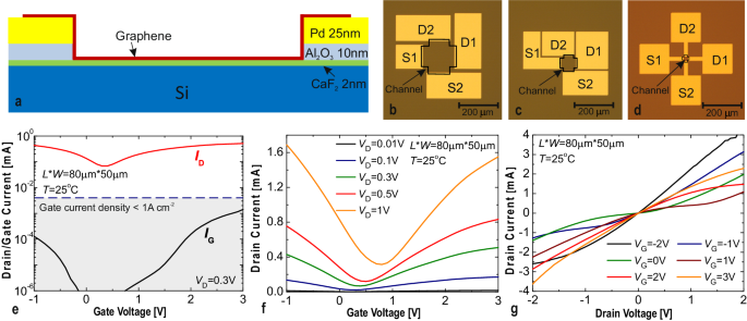
Graphene is a promising material for applications as a channel in graphene field-effect transistors (GFETs) which may be used as a building block for optoelectronics, high-frequency devices and sensors. However, these devices require gate insulators which ideally should form atomically flat interfaces with graphene and at the same time contain small densities of traps to maintain high device stability. Previously used amorphous oxides, such as SiO2 and Al2O3, however, typically suffer from oxide dangling bonds at the interface, high surface roughness and numerous border oxide traps. In order to address these challenges, here we use 2 nm thick epitaxial CaF2 as a gate insulator in GFETs. By analyzing device-to-device variability for about 200 devices fabricated in two batches, we find that tens of them show similar gate transfer characteristics. Our statistical analysis of the hysteresis up to 175oC has revealed that while an ambient-sensitive counterclockwise hysteresis can be present in some devices, the dominant mechanism is thermally activated charge trapping by border defects in CaF2 which results in the conventional clockwise hysteresis. We demonstrate that both the hysteresis and bias-temperature instabilities in our GFETs with CaF2 are comparable to similar devices with SiO2 and Al2O3. In particular, we achieve a small hysteresis below 0.01 V for equivalent oxide thickness (EOT) of about 1 nm at the electric fields up to 15 MV cm−1 and sweep times in the kilosecond range. Thus, our results demonstrate that crystalline CaF2 is a promising insulator for highly-stable GFETs.
中文翻译:
具有薄外延 CaF2 绝缘体的石墨烯场效应晶体管的可变性和高温可靠性
石墨烯是一种很有前途的材料,可用作石墨烯场效应晶体管(GFET)的通道,可用作光电子、高频器件和传感器的构建块。然而,这些器件需要栅极绝缘体,理想情况下栅极绝缘体应与石墨烯形成原子级平坦的界面,同时包含小密度的陷阱以保持器件的高稳定性。然而,先前使用的无定形氧化物,例如SiO 2和Al 2 O 3,通常遭受界面处的氧化物悬空键、高表面粗糙度和大量边界氧化物陷阱的困扰。为了应对这些挑战,这里我们使用 2 nm 厚的外延 CaF 2作为 GFET 中的栅极绝缘体。通过分析两批制造的约 200 个器件的器件间差异,我们发现其中数十个器件表现出相似的栅极传输特性。我们对高达 175 o C 的磁滞现象的统计分析表明,虽然某些器件中可能存在环境敏感的逆时针磁滞现象,但主要机制是 CaF 2中边界缺陷的热激活电荷俘获,这会导致传统的顺时针磁滞现象。我们证明,使用 CaF 2 的GFET 的磁滞和偏置温度不稳定性与使用 SiO 2和 Al 2 O 3的类似器件相当。特别是,我们在高达 15 MV cm -1的电场和千秒范围内的扫描时间下,对于约 1 nm 的等效氧化物厚度 (EOT),实现了低于 0.01 V 的小磁滞。因此,我们的结果表明,晶体 CaF 2是一种有前途的高稳定 GFET 绝缘体。


 京公网安备 11010802027423号