当前位置:
X-MOL 学术
›
Nanoscale Horiz.
›
论文详情
Our official English website, www.x-mol.net, welcomes your feedback! (Note: you will need to create a separate account there.)
Unraveling the origins of the coexisting localized-interfacial mechanism in oxide-based memristors in CMOS-integrated synaptic device implementations
Nanoscale Horizons ( IF 9.7 ) Pub Date : 2024-03-07 , DOI: 10.1039/d3nh00554b Eng Kang Koh 1, 2 , Putu Andhita Dananjaya 1 , Han Yin Poh 1, 2 , Lingli Liu 1 , Calvin Xiu Xian Lee 1, 2 , Jia Rui Thong 1, 2 , Young Seon You 2 , Wen Siang Lew 1
Nanoscale Horizons ( IF 9.7 ) Pub Date : 2024-03-07 , DOI: 10.1039/d3nh00554b Eng Kang Koh 1, 2 , Putu Andhita Dananjaya 1 , Han Yin Poh 1, 2 , Lingli Liu 1 , Calvin Xiu Xian Lee 1, 2 , Jia Rui Thong 1, 2 , Young Seon You 2 , Wen Siang Lew 1
Affiliation
|
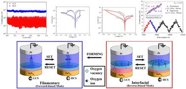
The forefront of neuromorphic research strives to develop devices with specific properties, i.e., linear and symmetrical conductance changes under external stimuli. This is paramount for neural network accuracy when emulating a biological synapse. A parallel exploration of resistive memory as a replacement for conventional computing memory ensues. In search of a holistic solution, the proposed memristive device in this work is uniquely poised to address this elusive gap as a unified memory solution. Opposite biasing operations are leveraged to achieve stable abrupt and gradual switching characteristics within a single device, addressing the demands for lower latency and energy consumption for binary switching applications, and graduality for neuromorphic computing applications. We evaluated the underlying principles of both switching modes, attributing the anomalous gradual switching to the modulation of oxygen-deficient layers formed between the active electrode and oxide switching layer. The memristive cell (1R) was integrated with 40 nm transistor technology (1T) to form a 1T–1R memory cell, demonstrating a switching speed of 50 ns with a pulse amplitude of ±2.5 V in its forward-biased mode. Applying pulse trains of 20 ns to 490 ns in the reverse-biased mode exhibited synaptic weight properties, obtaining a nonlinearity (NL) factor of <0.5 for both potentiation and depression. The devices in both modes also demonstrated an endurance of >106 cycles, and their conductance states were also stable under temperature stress at 85 °C for 104 s. With the duality of the two switching modes, our device can be used for both memory and synaptic weight-storing applications.
中文翻译:

揭示 CMOS 集成突触器件实现中氧化物忆阻器共存局部界面机制的起源
神经形态研究的前沿致力于开发具有特定特性的设备,即在外部刺激下产生线性和对称的电导变化。在模拟生物突触时,这对于神经网络的准确性至关重要。随之而来的是电阻式存储器作为传统计算存储器的替代品的并行探索。为了寻找整体解决方案,这项工作中提出的忆阻器件独特地准备作为统一的内存解决方案来解决这一难以捉摸的差距。利用相反的偏置操作来在单个器件内实现稳定的突然和渐进的开关特性,满足二进制开关应用的低延迟和能耗以及神经形态计算应用的渐进性的需求。我们评估了两种切换模式的基本原理,将异常逐渐切换归因于活性电极和氧化物切换层之间形成的缺氧层的调制。忆阻单元 (1R) 与 40 nm 晶体管技术 (1T) 集成,形成 1T–1R 存储单元,在正向偏置模式下,开关速度为 50 ns,脉冲幅度为 ±2.5 V。在反向偏置模式下应用 20 ns 至 490 ns 的脉冲序列表现出突触权重特性,增强和抑制的非线性 (NL) 因子均小于 0.5。两种模式下的器件还表现出>10 6 个循环的耐久性,并且它们的电导状态在85°C的温度应力下也稳定10 4 s。凭借两种开关模式的双重性,我们的设备可用于记忆和突触权重存储应用。
更新日期:2024-03-07
中文翻译:
揭示 CMOS 集成突触器件实现中氧化物忆阻器共存局部界面机制的起源
神经形态研究的前沿致力于开发具有特定特性的设备,即在外部刺激下产生线性和对称的电导变化。在模拟生物突触时,这对于神经网络的准确性至关重要。随之而来的是电阻式存储器作为传统计算存储器的替代品的并行探索。为了寻找整体解决方案,这项工作中提出的忆阻器件独特地准备作为统一的内存解决方案来解决这一难以捉摸的差距。利用相反的偏置操作来在单个器件内实现稳定的突然和渐进的开关特性,满足二进制开关应用的低延迟和能耗以及神经形态计算应用的渐进性的需求。我们评估了两种切换模式的基本原理,将异常逐渐切换归因于活性电极和氧化物切换层之间形成的缺氧层的调制。忆阻单元 (1R) 与 40 nm 晶体管技术 (1T) 集成,形成 1T–1R 存储单元,在正向偏置模式下,开关速度为 50 ns,脉冲幅度为 ±2.5 V。在反向偏置模式下应用 20 ns 至 490 ns 的脉冲序列表现出突触权重特性,增强和抑制的非线性 (NL) 因子均小于 0.5。两种模式下的器件还表现出>10 6 个循环的耐久性,并且它们的电导状态在85°C的温度应力下也稳定10 4 s。凭借两种开关模式的双重性,我们的设备可用于记忆和突触权重存储应用。


 京公网安备 11010802027423号