当前位置:
X-MOL 学术
›
Adv. Electron. Mater.
›
论文详情
Our official English website, www.x-mol.net, welcomes your feedback! (Note: you will need to create a separate account there.)
Direct Observation of Semimetal Contact Induced Charge Doping and Strain Effect in CVD‐Grown Monolayer MoS2 Transistors
Advanced Electronic Materials ( IF 6.2 ) Pub Date : 2024-03-05 , DOI: 10.1002/aelm.202300820 Xuewei Feng 1 , Zhi Gen Yu 2 , Haoyue Guo 3 , Yida Li 3 , Yong‐Wei Zhang 2 , Kah‐Wee Ang 4
Advanced Electronic Materials ( IF 6.2 ) Pub Date : 2024-03-05 , DOI: 10.1002/aelm.202300820 Xuewei Feng 1 , Zhi Gen Yu 2 , Haoyue Guo 3 , Yida Li 3 , Yong‐Wei Zhang 2 , Kah‐Wee Ang 4
Affiliation
|
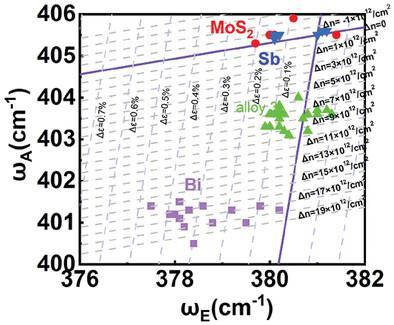
Two‐dimensional Materials (2DMs) offer significant promise for advancing device miniaturization and extending Moore's law. Despite the challenges posed by high contact resistance in transistors, recent discoveries highlight semimetals as an effective approach for achieving ohmic contact with near‐quantum‐limit contact resistance. The energy band hybridization between semimetal and MoS2 is found to create degenerate states and heavily doped contact, which is proposed as the underlying mechanism responsible for reducing contact resistance. However, a quantitative and comprehensive characterization of the semimetal‐MoS2 interface is lacking, leaving the physical interactions elusive. This study reveals that semimetals induce n ‐type doping and tensile strain in monolayer MoS2 grown using CVD, which serve as the contact resistance and mobility boosters. Among the semimetals investigated, including Bismuth (Bi), Antimony (Sb), and their alloy, Bi results in the highest electron doping of 2 × 1013 cm−2 and a 0.5% tensile strain, leading to reduced contact resistance and enhanced mobility. First‐principles calculations and spectroscopy measurements unveil the impact of electron doping and strain in MoS2 , and the thermal effects are subsequently explored. This research underscores the potential of semimetals in boosting device performance and lays the foundation for reducing contact resistance in transistors made from 2D materials.
中文翻译:

直接观察 CVD 生长的单层 MoS2 晶体管中的半金属接触感应电荷掺杂和应变效应
二维材料 (2DM) 为推进设备小型化和扩展摩尔定律提供了重要前景。尽管晶体管的高接触电阻带来了挑战,但最近的发现强调半金属是实现具有接近量子极限接触电阻的欧姆接触的有效方法。半金属与MoS2的能带杂化2 发现会产生简并态和重掺杂接触,这被认为是降低接触电阻的潜在机制。然而,半金属-MoS2的定量和综合表征2 缺乏界面,导致物理交互难以捉摸。这项研究表明半金属会诱导n 单层MoS中的‐型掺杂和拉伸应变2 使用 CVD 生长,充当接触电阻和迁移率增强器。在所研究的半金属中,包括铋 (Bi)、锑 (Sb) 及其合金,Bi 的电子掺杂量最高,为 2 × 10¹³ 厘米−2 和 0.5% 的拉伸应变,从而降低接触电阻并增强迁移率。第一性原理计算和光谱测量揭示了 MoS2 中电子掺杂和应变的影响2 ,随后探讨了热效应。这项研究强调了半金属在提高器件性能方面的潜力,并为降低二维材料晶体管的接触电阻奠定了基础。
更新日期:2024-03-05
中文翻译:
直接观察 CVD 生长的单层 MoS2 晶体管中的半金属接触感应电荷掺杂和应变效应
二维材料 (2DM) 为推进设备小型化和扩展摩尔定律提供了重要前景。尽管晶体管的高接触电阻带来了挑战,但最近的发现强调半金属是实现具有接近量子极限接触电阻的欧姆接触的有效方法。半金属与MoS2的能带杂化


 京公网安备 11010802027423号