当前位置:
X-MOL 学术
›
Adv. Electron. Mater.
›
论文详情
Our official English website, www.x-mol.net, welcomes your feedback! (Note: you will need to create a separate account there.)
Plasma and Gas‐based Semiconductor Technologies for 2D Materials with Computational Simulation & Electronic Applications
Advanced Electronic Materials ( IF 6.2 ) Pub Date : 2024-02-23 , DOI: 10.1002/aelm.202300835 Changmin Kim 1 , Muyoung Kim 1 , Seongho Kim 1, 2 , Minji Kang 1, 2 , Min Sup Choi 2 , Hyeong‐U Kim 1
Advanced Electronic Materials ( IF 6.2 ) Pub Date : 2024-02-23 , DOI: 10.1002/aelm.202300835 Changmin Kim 1 , Muyoung Kim 1 , Seongho Kim 1, 2 , Minji Kang 1, 2 , Min Sup Choi 2 , Hyeong‐U Kim 1
Affiliation
|
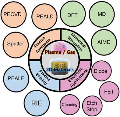
The technique of plasma processing is beneficial for wafer cleaning and precision etching of integrated circuits and essential in manufacture of advanced semiconductor devices with unmatched perfection. Research on two‐dimensional (2D) materials, such as transition metal dichalcogenides(TMDs), offers a promising solution to the challenges in semiconductor miniaturization. TMDs, with their atomic layer thicknesses and silicon‐like bandgaps, can be integrated using existing plasma systems. Different 2D crystal structures, such as 1T and 2H configurations, exhibit distinctive properties. Computational approaches are also developed to provide guidelines for controlled synthesis and etching of large‐scale and high‐quality 2D materials. Plasma/gas‐surface interactions during the synthesis, etching, and phase transformation of 2D materials are explored using atomistic simulations such as density functional theory and molecular dynamics. The reaction energetics, chemical species, and associated kinetics are discovered in the simulation study. These results decipher various mechanisms of 2D materials processing at the microscopic scale and predict certain optimal process parameters. Plasma/gas‐based semiconductor technologies are crucial in electronics because they enable production of advanced semiconductors. Plasma/gas etching allows precise and selective removal of material and plasma‐enhanced chemical vapor deposition enhances chemical reactions for efficient film deposition; therefore, these processes are majorly important for harnessing 2D materials in electronic applications.
中文翻译:

用于二维材料的等离子体和气体半导体技术以及计算模拟和电子应用
等离子体处理技术有利于晶圆清洗和集成电路的精密蚀刻,对于制造完美的先进半导体器件至关重要。二维(2D)材料(例如过渡金属二硫属化物(TMD))的研究为解决半导体小型化的挑战提供了一种有前景的解决方案。TMD 具有原子层厚度和类似硅的带隙,可以使用现有的等离子体系统进行集成。不同的 2D 晶体结构,例如 1T 和 2H 配置,表现出独特的特性。还开发了计算方法,为大规模和高质量二维材料的受控合成和蚀刻提供指导。使用密度泛函理论和分子动力学等原子模拟来探索二维材料的合成、蚀刻和相变过程中的等离子体/气体表面相互作用。模拟研究中发现了反应能量学、化学物质和相关动力学。这些结果破译了微观尺度上二维材料加工的各种机制,并预测了某些最佳工艺参数。基于等离子体/气体的半导体技术在电子领域至关重要,因为它们可以生产先进的半导体。等离子/气体蚀刻可以精确、选择性地去除材料,等离子增强化学气相沉积可以增强化学反应,实现高效的薄膜沉积;因此,这些工艺对于在电子应用中利用二维材料非常重要。
更新日期:2024-02-23
中文翻译:
用于二维材料的等离子体和气体半导体技术以及计算模拟和电子应用
等离子体处理技术有利于晶圆清洗和集成电路的精密蚀刻,对于制造完美的先进半导体器件至关重要。二维(2D)材料(例如过渡金属二硫属化物(TMD))的研究为解决半导体小型化的挑战提供了一种有前景的解决方案。TMD 具有原子层厚度和类似硅的带隙,可以使用现有的等离子体系统进行集成。不同的 2D 晶体结构,例如 1T 和 2H 配置,表现出独特的特性。还开发了计算方法,为大规模和高质量二维材料的受控合成和蚀刻提供指导。使用密度泛函理论和分子动力学等原子模拟来探索二维材料的合成、蚀刻和相变过程中的等离子体/气体表面相互作用。模拟研究中发现了反应能量学、化学物质和相关动力学。这些结果破译了微观尺度上二维材料加工的各种机制,并预测了某些最佳工艺参数。基于等离子体/气体的半导体技术在电子领域至关重要,因为它们可以生产先进的半导体。等离子/气体蚀刻可以精确、选择性地去除材料,等离子增强化学气相沉积可以增强化学反应,实现高效的薄膜沉积;因此,这些工艺对于在电子应用中利用二维材料非常重要。


 京公网安备 11010802027423号