当前位置:
X-MOL 学术
›
Adv. Electron. Mater.
›
论文详情
Our official English website, www.x-mol.net, welcomes your feedback! (Note: you will need to create a separate account there.)
Graphene-Based Lateral Heterojunctions for 2D Integrated Circuits
Advanced Electronic Materials ( IF 6.2 ) Pub Date : 2024-02-16 , DOI: 10.1002/aelm.202300761 Mohd.Musaib Haidari 1 , Dong Jin Jang 1 , Duhee Yoon 2, 3 , Hakseong Kim 4 , Hong Kyw Choi 5 , Yoonsik Yi 5 , Jin Hong Kim 1 , Jin‐Yong Ko 1 , Dooho Lee 6 , Eun Hee Kee 1 , Hu Young Jeong 7 , Jeong Young Park 6 , Bae Ho Park 1 , Jin Sik Choi 1
Advanced Electronic Materials ( IF 6.2 ) Pub Date : 2024-02-16 , DOI: 10.1002/aelm.202300761 Mohd.Musaib Haidari 1 , Dong Jin Jang 1 , Duhee Yoon 2, 3 , Hakseong Kim 4 , Hong Kyw Choi 5 , Yoonsik Yi 5 , Jin Hong Kim 1 , Jin‐Yong Ko 1 , Dooho Lee 6 , Eun Hee Kee 1 , Hu Young Jeong 7 , Jeong Young Park 6 , Bae Ho Park 1 , Jin Sik Choi 1
Affiliation
|
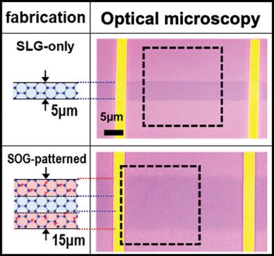
A method for patterning single-layer graphene (SLG) and single-layer oxidized graphene (SOG) within a continuous atomic layer to form lateral heterojunctions is presented. Raman spectroscopy is employed to investigate the evolution of defect-related Raman peaks during excimer-UV irradiation, facilitating the identification of structural changes and defect formation processes. Electrical transport measurements reveal that SOG-patterned field-effect transistors (FETs) exhibit varying characteristics depending on the degree of oxidation, thus offering the potential to tailor the electrical properties of graphene devices for specific requirements. Scanning Kelvin probe microscopy measurements reveal the surface potential and work function of the SOG regions compared with those of SLG. The effective functionality of the SOG pattern to operate as a resistor, allowing control of the electrical conductivity in the SOG-patterned SLG channels, is demonstrated. This capability restricts the current flow while preserving the pristine electrical properties of the graphene channel. Moreover, the SOG pattern can serve as a potential barrier to constructing SLG-SOG-patterned integrated circuits, providing exciting opportunities for engineering advanced electronic components. This breakthrough in graphene devices simplifies the fabrication process of graphene-based FETs and provides the foundation for developing atomically thin integrated circuits for a wide range of applications.
中文翻译:

用于二维集成电路的石墨烯横向异质结
提出了一种在连续原子层内图案化单层石墨烯(SLG)和单层氧化石墨烯(SOG)以形成横向异质结的方法。拉曼光谱用于研究准分子紫外线照射期间与缺陷相关的拉曼峰的演变,有助于识别结构变化和缺陷形成过程。电传输测量表明,SOG 图案的场效应晶体管 (FET) 根据氧化程度表现出不同的特性,从而提供了根据特定要求定制石墨烯器件电性能的潜力。扫描开尔文探针显微镜测量揭示了 SOG 区域与 SLG 区域的表面电势和功函数。演示了 SOG 图案作为电阻器运行的有效功能,允许控制 SOG 图案 SLG 通道中的电导率。这种能力限制了电流,同时保留了石墨烯通道的原始电特性。此外,SOG图案可以作为构建SLG-SOG图案集成电路的潜在障碍,为设计先进电子元件提供令人兴奋的机会。石墨烯器件的这一突破简化了基于石墨烯的 FET 的制造工艺,并为开发适用于各种应用的原子薄集成电路奠定了基础。
更新日期:2024-02-16
中文翻译:
用于二维集成电路的石墨烯横向异质结
提出了一种在连续原子层内图案化单层石墨烯(SLG)和单层氧化石墨烯(SOG)以形成横向异质结的方法。拉曼光谱用于研究准分子紫外线照射期间与缺陷相关的拉曼峰的演变,有助于识别结构变化和缺陷形成过程。电传输测量表明,SOG 图案的场效应晶体管 (FET) 根据氧化程度表现出不同的特性,从而提供了根据特定要求定制石墨烯器件电性能的潜力。扫描开尔文探针显微镜测量揭示了 SOG 区域与 SLG 区域的表面电势和功函数。演示了 SOG 图案作为电阻器运行的有效功能,允许控制 SOG 图案 SLG 通道中的电导率。这种能力限制了电流,同时保留了石墨烯通道的原始电特性。此外,SOG图案可以作为构建SLG-SOG图案集成电路的潜在障碍,为设计先进电子元件提供令人兴奋的机会。石墨烯器件的这一突破简化了基于石墨烯的 FET 的制造工艺,并为开发适用于各种应用的原子薄集成电路奠定了基础。


 京公网安备 11010802027423号