Journal of Materiomics ( IF 9.4 ) Pub Date : 2023-11-23 , DOI: 10.1016/j.jmat.2023.11.002 Fulin Zhang , Songtao Fan , Yingxu Zhu , Wendie Chen , Bing Liu , Yuguo Yang , Limei Zheng , Yuanyuan Zhang , Xianshun Lv , Xuping Wang
|
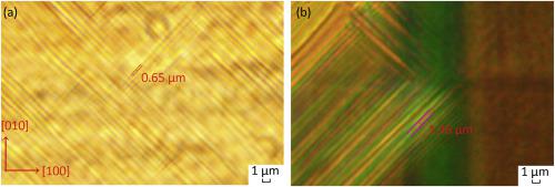
As a class of solid solution material, K(Ta,Nb)O3 (KTN) single crystals have attracted significant interest due to their excellent piezoelectric and electro-optic performance. In this study, the piezoelectric properties of KTN were improved through Cu doping. Utilizing the advantages of composition-regulating phase transition, a large, high-quality Cu:KTN crystal measuring 30 mm × 25 mm × 20 mm in size was grown using the improved top seeded solution growth method. Cu-doped KTN exhibited better piezoelectric properties than pure KTN, and the full matrix parameters were investigated. Excellent dielectric, piezoelectric, and electromechanical coupling responses ( 2,136, d33∼303 pC/N, kt∼0.515, and k33∼0.672) were successfully obtained. To realize the optimized orientation of the piezoelectric properties, the orientation dependence of the single domain properties was investigated, and the mechanism of Cu doping to improve piezoelectric properties was explored. We found that 0.36% (in mass) Cu doped crystal consisted of A-site substitution, following ferroelectric and domain analysis. The small ferroelectric domain sizes led to a large domain wall mobility rate and high domain wall density, which contributed to high piezoelectric properties. This work revealed the effect of A-position doping on piezoelectric properties and provided a theoretical and experimental foundation for the performance optimization of KTN-based materials.
中文翻译:
Cu掺杂K(Ta,Nb)O3单晶的增强压电性
作为一类固溶体材料,K(Ta,Nb)O 3 (KTN)单晶因其优异的压电和电光性能而引起了人们的广泛关注。在这项研究中,KTN的压电性能通过Cu掺杂得到了改善。利用成分调节相变的优势,采用改进的顶晶溶液生长方法生长出尺寸为 30 mm × 25 mm × 20 mm 的大型高质量 Cu:KTN 晶体。掺杂铜的 KTN 表现出比纯 KTN 更好的压电性能,并且对全基体参数进行了研究。优异的介电、压电和机电耦合响应(成功获得了2,136、d 33 ∼303 pC/N、k t ∼0.515 和k 33 ∼0.672)。为了实现压电性能的优化取向,研究了单畴性能的取向依赖性,并探索了Cu掺杂改善压电性能的机制。经过铁电和磁畴分析,我们发现 0.36%(质量)的 Cu 掺杂晶体由 A 位取代组成。小的铁电畴尺寸导致大的畴壁迁移率和高的畴壁密度,这有助于产生高压电性能。该工作揭示了A位掺杂对压电性能的影响,为KTN基材料的性能优化提供了理论和实验基础。


 京公网安备 11010802027423号