npj 2D Materials and Applications ( IF 9.7 ) Pub Date : 2023-10-19 , DOI: 10.1038/s41699-023-00434-9 Fangzhu Xiong , Jie Sun , Penghao Tang , Weiling Guo , Yibo Dong , Zaifa Du , Shiwei Feng , Xuan Li
|
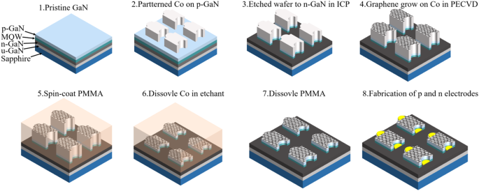
A technique for the transfer-free growth of 2-inch wafer-scale patterned graphene directly on GaN LED epilayers is introduced. High-quality graphene as transparent electrodes and heat spreaders is synthesized directly on GaN by PECVD at only 600 °C deposition temperature and within 3 min growth time. Co acts as both the catalyst for graphene growth and the dry etching mask for GaN mesas, which greatly improves the efficiency of the semiconductor device process. Elegantly, the graphene growth is in accordance with the shape of Co, which offers a lithography-free patterning technique of the graphene. Afterward, using our penetration etching method through the PMMA and graphene layers, the Co is peacefully removed, and in-situ Ohmic contact is achieved between the graphene and p-GaN where the contact resistivity is only 0.421 Ω cm2. The graphene sheet resistance is as low as 631.2 Ω sq−1. The device is also superior to the counterpart graphene-free LED in terms of heat spreading behavior, as evidenced by the lower junction temperature and thermal resistance. Most importantly, the developed technique produces graphene with excellent performance and is intrinsically more scalable, controllable, and semiconductor industry compatible than traditionally transferred graphene.
中文翻译:
无转移快速生长 2 英寸晶圆级图案化石墨烯作为 GaN LED 的透明导电电极和散热器
介绍了直接在 GaN LED 外延层上无转移生长 2 英寸晶圆级图案化石墨烯的技术。作为透明电极和散热器的高质量石墨烯是通过 PECVD 直接在 GaN 上合成的,沉积温度仅为 600 °C,生长时间为 3 分钟。Co既充当石墨烯生长的催化剂,又充当GaN台面的干法刻蚀掩模,大大提高了半导体器件工艺的效率。优雅的是,石墨烯的生长与Co的形状一致,这提供了石墨烯的免光刻图案化技术。然后,使用我们的渗透蚀刻方法穿过PMMA和石墨烯层,将Co平静地去除,并在石墨烯和p-GaN之间实现原位欧姆接触,接触电阻率仅为0.421 Ω cm 2。石墨烯薄层电阻低至631.2Ω sq -1。该器件在散热行为方面也优于对应的无石墨烯 LED,结温和热阻较低就证明了这一点。最重要的是,所开发的技术生产出性能优异的石墨烯,并且本质上比传统转移石墨烯更具可扩展性、可控性和半导体行业兼容性。


 京公网安备 11010802027423号