Journal of Materials Science & Technology ( IF 11.2 ) Pub Date : 2023-06-02 , DOI: 10.1016/j.jmst.2023.05.007 Ming Deng , Ziqing Li , Xiaolei Deng , Ying Hu , Xiaosheng Fang
|
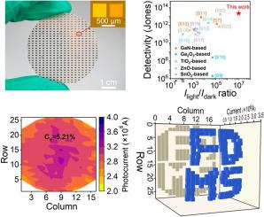
Large-scale growth and heterogeneous integration with existing semiconductors are the main obstacles to the application of metal halide perovskites in optoelectronics. Herein, a universal vacuum evaporation strategy is presented to prepare copper halide films with wafer-scale spatial homogeneity. Benefiting from the electric field manipulation method, the built-in electric fields are optimized and further boost the self-powered UV photodetecting performances of common wide-bandgap semiconductors by more than three orders of magnitude. Furthermore, with effective modulation of the interfacial charge dynamics, the as-fabricated GaN-substrate heterojunction photodetector demonstrates an ultrahigh on/off ratio exceeding 107, an impressive responsivity of up to 256 mA W–1, and a remarkable detectivity of 2.16 × 10¹³ Jones at 350 nm, 0 V bias. Additionally, the device exhibits an ultrafast response speed (tr / td = 716 ns / 1.30 ms), an ultra-narrow photoresponse spectrum with an FWHM of 18 nm and outstanding continuous operational stability as well as long-term stability. Subsequently, a 372-pixel light-powered imaging sensor array with the coefficient of variation of photocurrents reducing to 5.20% is constructed, which demonstrates exceptional electrical homogeneity, operational reliability, and UV imaging capability. This strategy provides an efficient way for large-scale integration of metal halide perovskites with commercial semiconductors for miniature optoelectronic devices.
中文翻译:
具有超高稳定性和均匀性的自供电无铅金属卤化物紫外光电探测器的晶圆级异构集成
大规模生长和与现有半导体的异质集成是金属卤化物钙钛矿在光电领域应用的主要障碍。在此,提出了一种通用的真空蒸发策略来制备具有晶圆级空间均匀性的卤化铜薄膜。受益于电场操纵方法,优化了内置电场,进一步将普通宽带隙半导体的自供电紫外光电探测性能提高了三个数量级以上。此外,通过有效调制界面电荷动力学,制造的 GaN 衬底异质结光电探测器展示了超过 10 7 的超高开/关比,令人印象深刻的响应度高达 256 mA W –1,以及在 350 nm、0 V 偏压下 2.16 × 10 13琼斯的显着检测率。此外,该器件还具有超快响应速度(t r / t d = 716 ns / 1.30 ms)、FWHM 为 18 nm 的超窄光响应光谱以及出色的连续运行稳定性和长期稳定性。随后,构建了光电流变异系数降至 5.20% 的 372 像素光驱动成像传感器阵列,展示了出色的电均匀性、运行可靠性和紫外成像能力。该策略为金属卤化物钙钛矿与用于微型光电器件的商业半导体的大规模集成提供了一种有效的方法。


 京公网安备 11010802027423号