Journal of Alloys and Compounds ( IF 6.2 ) Pub Date : 2023-06-01 , DOI: 10.1016/j.jallcom.2023.170617 Binita Tongbram , Vidya P. Deviprasad , Amit Vitthal Kumbhar , Saumya Sengupta , Subhananda Chakrabarti
|
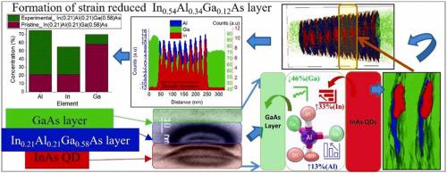
We demonstrate the correlative research on the multi-stacked vertically coupled InAs quantum dots (VCQDs) capped by 15 nm combinational capping layer of In(0.21)Al(0.21)Ga(0.58)As and GaAs layer through Atom probe tomography (APT), Transmission Electron Microscopy (TEM), Secondary Ion Mass Spectroscopy (SIMS), High-Resolution X-Ray Diffraction (HRXRD) and Reciprocal Space Mapping (RSM). From the comparative studies, we observed a strain reduction of ~ 2.3 ±0.05% in the system, leading to the formation of strain-reduced (SR) In0.54Al0.34Ga0.12As layer with a lattice constant of 5.88 Å, which will work as a shielding layer. We found that the middle portion of the 3rd to 8th layer QDs structure was constant in size, shape, composition, and density, which enhances the carrier confinement in QDs. The computed strain energy values contributed to the overall growth structure of the 30 - layers VCQDs were recorded to be 2.2 meV/atoms. We report the detailed analogy of the in-out flow of In/Ga adatoms in the In0.54Al0.34Ga0.12As layer leading to the evolution of fully developed bigger InAs QDs size. To support the APT results, we also present the outcomes studies of the HRXRD Out-plane and In-Plane symmetric RSM experiment at (002), (004), and (006) reflections to investigate the compressive strain contribution in the SR In0.54Al0.34Ga0.12As shielding layer. This 30-layer VCQDs structure can be employed to fabricate high thermal stability operating at 1.3µm O-band telecom Single Photon Sources (SPSs).
中文翻译:
用于 O 波段电信单光子源的垂直耦合 QD 阵列的应变降低 In0.54Al0.34Ga0.12As 层的形成
我们通过原子探针断层扫描 (APT) 展示了对由In (0.21) Al (0.21) Ga (0.58) As 和 GaAs 层的 15 nm 组合覆盖层覆盖的多层堆叠垂直耦合 InAs 量子点 (VCQD) 的相关研究,透射电子显微镜 (TEM)、二次离子质谱 (SIMS)、高分辨率 X 射线衍射 (HRXRD) 和倒易空间映射 (RSM)。从比较研究中,我们观察到系统中应变减少了 ~ 2.3 ±0.05%,导致形成应变减少 (SR) In 0.54 Al 0.34 Ga 0.12 As层,晶格常数为 5.88 Å,它将用作屏蔽层。我们发现第3至第 8层QD 结构的中间部分在尺寸、形状、组成和密度上是恒定的,这增强了 QD 中的载流子限制。计算出的应变能值对 30 层 VCQD 的整体生长结构有贡献,记录为 2.2 meV/原子。我们报告了 In/Ga 吸附原子在 In 0.54 Al 0.34 Ga 0.12中进出流动的详细类比作为导致完全开发更大尺寸 InAs QD 的层。为了支持 APT 结果,我们还介绍了 (002)、(004) 和 (006) 反射的 HRXRD 面外和面内对称 RSM 实验的结果研究,以研究 SR In 0.54中的压应变贡献Al 0.34 Ga 0.12作为屏蔽层。这种 30 层 VCQD 结构可用于制造在 1.3µm O 波段电信单光子源 (SPS) 下运行的高热稳定性。


 京公网安备 11010802027423号