当前位置:
X-MOL 学术
›
Nano Lett.
›
论文详情
Our official English website, www.x-mol.net, welcomes your feedback! (Note: you will need to create a separate account there.)
Atomic-Resolution Spectrum Imaging of Semiconductor Nanowires
Nano Letters ( IF 10.8 ) Pub Date : 2017-11-13 00:00:00 , DOI: 10.1021/acs.nanolett.7b03929 Reza R. Zamani 1 , Fredrik S. Hage 2 , Sebastian Lehmann 1 , Quentin M. Ramasse 2 , Kimberly A. Dick 1, 3
Nano Letters ( IF 10.8 ) Pub Date : 2017-11-13 00:00:00 , DOI: 10.1021/acs.nanolett.7b03929 Reza R. Zamani 1 , Fredrik S. Hage 2 , Sebastian Lehmann 1 , Quentin M. Ramasse 2 , Kimberly A. Dick 1, 3
Affiliation
|
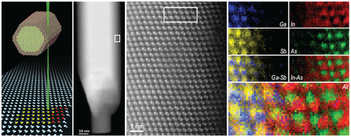
Over the past decade, III–V heterostructure nanowires have attracted a surge of attention for their application in novel semiconductor devices such as tunneling field-effect transistors (TFETs). The functionality of such devices critically depends on the specific atomic arrangement at the semiconductor heterointerfaces. However, most of the currently available characterization techniques lack sufficient spatial resolution to provide local information on the atomic structure and composition of these interfaces. Atomic-resolution spectrum imaging by means of electron energy-loss spectroscopy (EELS) in the scanning transmission electron microscope (STEM) is a powerful technique with the potential to resolve structure and chemical composition with sub-angstrom spatial resolution and to provide localized information about the physical properties of the material at the atomic scale. Here, we demonstrate the use of atomic-resolution EELS to understand the interface atomic arrangement in three-dimensional heterostructures in semiconductor nanowires. We observed that the radial interfaces of GaSb–InAs heterostructure nanowires are atomically abrupt, while the axial interface in contrast consists of an interfacial region where intermixing of the two compounds occurs over an extended spatial region. The local atomic configuration affects the band alignment at the interface and, hence, the charge transport properties of devices such as GaSb–InAs nanowire TFETs. STEM–EELS thus represents a very promising technique for understanding nanowire physical properties, such as differing electrical behavior across the radial and axial heterointerfaces of GaSb–InAs nanowires for TFET applications.
中文翻译:

半导体纳米线的原子分辨光谱成像
在过去的十年中,III–V异质结构纳米线因其在新型半导体器件(例如隧道效应晶体管(TFET))中的应用而引起了人们的关注。这样的设备的功能主要取决于半导体异质界面上的特定原子排列。但是,大多数当前可用的表征技术缺乏足够的空间分辨率,无法提供有关这些界面的原子结构和组成的局部信息。在扫描透射电子显微镜(STEM)中借助电子能量损失谱(EELS)进行原子分辨率光谱成像是一项强大的技术,具有解决亚埃空间分辨率的结构和化学成分并提供有关以下方面的局部信息的潜力材料在原子尺度上的物理性质。在这里,我们演示了使用原子分辨率EELS来了解半导体纳米线中三维异质结构中的界面原子排列。我们观察到,GaSb-InAs异质结构纳米线的径向界面在原子上是突变的,而轴向界面则由一个界面区域组成,在该界面区域中,两种化合物的混合发生在扩展的空间区域上。局部原子构型会影响界面处的能带对准,因此会影响GaSb-InAs纳米线TFET等器件的电荷传输性能。因此,STEM–EELS代表了一种非常有前途的技术,可用于理解纳米线的物理特性,例如用于TFET应用的GaSb–InAs纳米线的径向和轴向异质界面上的不同电行为。
更新日期:2017-11-14
中文翻译:
半导体纳米线的原子分辨光谱成像
在过去的十年中,III–V异质结构纳米线因其在新型半导体器件(例如隧道效应晶体管(TFET))中的应用而引起了人们的关注。这样的设备的功能主要取决于半导体异质界面上的特定原子排列。但是,大多数当前可用的表征技术缺乏足够的空间分辨率,无法提供有关这些界面的原子结构和组成的局部信息。在扫描透射电子显微镜(STEM)中借助电子能量损失谱(EELS)进行原子分辨率光谱成像是一项强大的技术,具有解决亚埃空间分辨率的结构和化学成分并提供有关以下方面的局部信息的潜力材料在原子尺度上的物理性质。在这里,我们演示了使用原子分辨率EELS来了解半导体纳米线中三维异质结构中的界面原子排列。我们观察到,GaSb-InAs异质结构纳米线的径向界面在原子上是突变的,而轴向界面则由一个界面区域组成,在该界面区域中,两种化合物的混合发生在扩展的空间区域上。局部原子构型会影响界面处的能带对准,因此会影响GaSb-InAs纳米线TFET等器件的电荷传输性能。因此,STEM–EELS代表了一种非常有前途的技术,可用于理解纳米线的物理特性,例如用于TFET应用的GaSb–InAs纳米线的径向和轴向异质界面上的不同电行为。


 京公网安备 11010802027423号