当前位置:
X-MOL 学术
›
Nano Lett.
›
论文详情
Our official English website, www.x-mol.net, welcomes your
feedback! (Note: you will need to create a separate account there.)
Mapping Free-Carriers in Multijunction Silicon Nanowires Using Infrared Near-Field Optical Microscopy
Nano Letters ( IF 9.6 ) Pub Date : 2017-10-30 00:00:00 , DOI: 10.1021/acs.nanolett.7b02340 Earl T. Ritchie 1 , David J. Hill 1 , Tucker M. Mastin 1 , Panfilo C. Deguzman 2 , James F. Cahoon 1 , Joanna M. Atkin 1
Nano Letters ( IF 9.6 ) Pub Date : 2017-10-30 00:00:00 , DOI: 10.1021/acs.nanolett.7b02340 Earl T. Ritchie 1 , David J. Hill 1 , Tucker M. Mastin 1 , Panfilo C. Deguzman 2 , James F. Cahoon 1 , Joanna M. Atkin 1
Affiliation
|
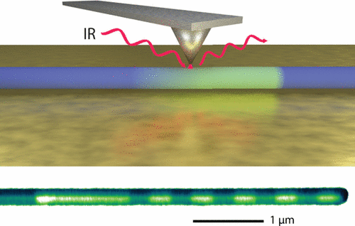
We report the use of infrared (IR) scattering-type scanning near-field optical microscopy (s-SNOM) as a nondestructive method to map free-carriers in axially modulation-doped silicon nanowires (SiNWs) with nanoscale spatial resolution. Using this technique, we can detect local changes in the electrically active doping concentration based on the infrared free-carrier response in SiNWs grown using the vapor–liquid–solid (VLS) method. We demonstrate that IR s-SNOM is sensitive to both p-type and n-type free-carriers for carrier densities above ∼1 × 1019 cm–3. We also resolve subtle changes in local conductivity properties, which can be correlated with growth conditions and surface effects. The use of s-SNOM is especially valuable in low mobility materials such as boron-doped p-type SiNWs, where optimization of growth has been difficult to achieve due to the lack of information on dopant distribution and junction properties. s-SNOM can be widely employed for the nondestructive characterization of nanostructured material synthesis and local electronic properties without the need for contacts or inert atmosphere.
中文翻译:

使用红外近场光学显微镜在多结硅纳米线中映射自由载流子
我们报告使用红外(IR)散射型扫描近场光学显微镜(s-SNOM)作为一种无损方法,以纳米级空间分辨率映射轴向调制掺杂的硅纳米线(SiNWs)中的自由载流子。使用这种技术,我们可以基于使用汽-液-固(VLS)方法生长的SiNW中的红外自由载流子响应,检测电活性掺杂浓度的局部变化。我们证明IR s-SNOM对p型和n型自由载子都敏感,其载流子密度约为〜1×10 19 cm –3。我们还解决了局部电导率特性的细微变化,这可能与生长条件和表面效应相关。s-SNOM在低迁移率材料(例如掺硼p型SiNW)中尤其有价值,由于缺乏关于掺杂剂分布和结性质的信息,难以实现生长的优化。s-SNOM可广泛用于纳米结构材料合成和局部电子特性的非破坏性表征,而无需接触或惰性气氛。
更新日期:2017-10-31
中文翻译:
使用红外近场光学显微镜在多结硅纳米线中映射自由载流子
我们报告使用红外(IR)散射型扫描近场光学显微镜(s-SNOM)作为一种无损方法,以纳米级空间分辨率映射轴向调制掺杂的硅纳米线(SiNWs)中的自由载流子。使用这种技术,我们可以基于使用汽-液-固(VLS)方法生长的SiNW中的红外自由载流子响应,检测电活性掺杂浓度的局部变化。我们证明IR s-SNOM对p型和n型自由载子都敏感,其载流子密度约为〜1×10 19 cm –3。我们还解决了局部电导率特性的细微变化,这可能与生长条件和表面效应相关。s-SNOM在低迁移率材料(例如掺硼p型SiNW)中尤其有价值,由于缺乏关于掺杂剂分布和结性质的信息,难以实现生长的优化。s-SNOM可广泛用于纳米结构材料合成和局部电子特性的非破坏性表征,而无需接触或惰性气氛。


 京公网安备 11010802027423号