Organic Electronics ( IF 2.7 ) Pub Date : 2017-10-10 , DOI: 10.1016/j.orgel.2017.10.010 C.P. Watson , E.M. Lopes , R.F. de Oliveira , N. Alves , J.A. Giacometti , D.M. Taylor
|
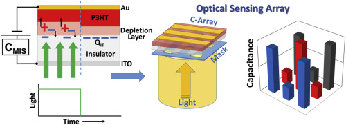
We report the results of an investigation into the contribution that trapping in interface states makes to the photovoltaic effect observed in organic phototransistors. To isolate this effect from other processes that occur in the transistor structure when under illumination, we focus attention on the photo-response of metal-insulator-semiconductor (MIS) capacitors - the core structure of transistors. The capacitors comprised poly(3-hexylthiophene), (P3HT), as the active semiconductor in combination with one of three insulators, namely, poly(amide-imide), (PAI), SU-8 photoresist and polysilsesquioxane (PSQ). Following initial characterization in the dark, the capacitor response was measured both during and after irradiation with light in the wavelength range 400–700 nm. Three different approaches were employed to study the photo-response, each providing a different insight into the processes occurring. Capacitance-voltage sweeps before, during and after illumination provided direct evidence supporting the view that the photovoltaic effect occurred as a result of electron trapping in interface states of density up to ∼2 × 1012 cm−2 in the P3HT/PAI combination but lower for SU-8 and PSQ. The dynamic photo-response, in which device capacitance was held constant by changing the applied bias, showed a fast component related to optically induced photoconduction in the semiconductor and a slower component reflecting the dynamics of interface electron trapping. Finally, photo-induced capacitance changes occurring with constant applied voltage were used to demonstrate a simple 3 × 3 imaging array.
中文翻译:
界面态对有机光电晶体管中光电效应的贡献:光电容测量和光学传感
我们报告了对界面态陷阱对有机光电晶体管中观察到的光伏效应做出贡献的调查结果。为了将这种影响与在光照下晶体管结构中发生的其他过程隔离开来,我们将注意力集中在金属-绝缘体-半导体(MIS)电容器的光响应-晶体管的核心结构上。电容器包括聚(3-己基噻吩)(P3HT),作为与三种绝缘体之一的活性半导体结合使用的三种绝缘体,即聚(酰胺-酰亚胺),(PAI),SU-8光致抗蚀剂和聚倍半硅氧烷(PSQ)。在黑暗中初步表征后,在波长范围为400-700 nm的光辐照期间和辐照后均测量了电容器的响应。采用了三种不同的方法来研究光响应,每一个都对发生的过程提供了不同的见解。电容电压在照明之前,期间和之后的扫描提供了直接的证据,支持以下观点:光伏效应是由于电子俘获的结果,其界面态的密度高达2×10P3HT / PAI组合中为12 cm -2,但SU-8和PSQ较低。通过改变施加的偏压使器件电容保持恒定的动态光响应,显示出与半导体中光感应光电导有关的快速成分,而反映界面电子俘获动力学的较慢成分。最后,在恒定施加电压下发生的光感应电容变化用于演示简单的3×3成像阵列。


 京公网安备 11010802027423号