当前位置:
X-MOL 学术
›
Adv. Mater.
›
论文详情
Our official English website, www.x-mol.net, welcomes your
feedback! (Note: you will need to create a separate account there.)
Highly Efficient Rubrene–Graphene Charge‐Transfer Interfaces as Phototransistors in the Visible Regime
Advanced Materials ( IF 27.4 ) Pub Date : 2017-09-25 , DOI: 10.1002/adma.201702993 Gareth F. Jones 1 , Rui M. Pinto 2 , Adolfo De Sanctis 1 , V. Karthik Nagareddy 1 , C. David Wright 1 , Helena Alves 3 , Monica F. Craciun 1 , Saverio Russo 1
Advanced Materials ( IF 27.4 ) Pub Date : 2017-09-25 , DOI: 10.1002/adma.201702993 Gareth F. Jones 1 , Rui M. Pinto 2 , Adolfo De Sanctis 1 , V. Karthik Nagareddy 1 , C. David Wright 1 , Helena Alves 3 , Monica F. Craciun 1 , Saverio Russo 1
Affiliation
|
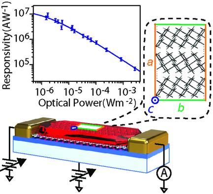
Atomically thin materials such as graphene are uniquely responsive to charge transfer from adjacent materials, making them ideal charge‐transport layers in phototransistor devices. Effective implementation of organic semiconductors as a photoactive layer would open up a multitude of applications in biomimetic circuitry and ultra‐broadband imaging but polycrystalline and amorphous thin films have shown inferior performance compared to inorganic semiconductors. Here, the long‐range order in rubrene single crystals is utilized to engineer organic‐semiconductor–graphene phototransistors surpassing previously reported photogating efficiencies by one order of magnitude. Phototransistors based upon these interfaces are spectrally selective to visible wavelengths and, through photoconductive gain mechanisms, achieve responsivity as large as 107 A W−1 and a detectivity of 9 × 10¹¹ Jones at room temperature. These findings point toward implementing low‐cost, flexible materials for amplified imaging at ultralow light levels.
中文翻译:

在可见光环境中作为光电晶体管的高效鲁宾-石墨烯电荷转移接口
原子稀薄的材料(例如石墨烯)对相邻材料的电荷转移具有独特的响应能力,使其成为光电晶体管器件中理想的电荷传输层。有效地将有机半导体用作光敏层将在仿生电路和超宽带成像中打开多种应用,但与无机半导体相比,多晶和非晶薄膜的性能较差。在这里,利用红荧烯单晶的远距离有序来工程化有机半导体-石墨烯光电晶体管,使其比以前报道的光闸效率高一个数量级。基于这些接口的光电晶体管对可见波长具有光谱选择性,并通过光电导增益机制实现高达10的响应度在室温下为7 AW -1,检测率为9×10 11 Jones。这些发现指向在低成本,柔性材料上实现超低光照水平下的放大成像。
更新日期:2017-09-25
中文翻译:
在可见光环境中作为光电晶体管的高效鲁宾-石墨烯电荷转移接口
原子稀薄的材料(例如石墨烯)对相邻材料的电荷转移具有独特的响应能力,使其成为光电晶体管器件中理想的电荷传输层。有效地将有机半导体用作光敏层将在仿生电路和超宽带成像中打开多种应用,但与无机半导体相比,多晶和非晶薄膜的性能较差。在这里,利用红荧烯单晶的远距离有序来工程化有机半导体-石墨烯光电晶体管,使其比以前报道的光闸效率高一个数量级。基于这些接口的光电晶体管对可见波长具有光谱选择性,并通过光电导增益机制实现高达10的响应度在室温下为7 AW -1,检测率为9×10 11 Jones。这些发现指向在低成本,柔性材料上实现超低光照水平下的放大成像。


 京公网安备 11010802027423号