Our official English website, www.x-mol.net, welcomes your
feedback! (Note: you will need to create a separate account there.)
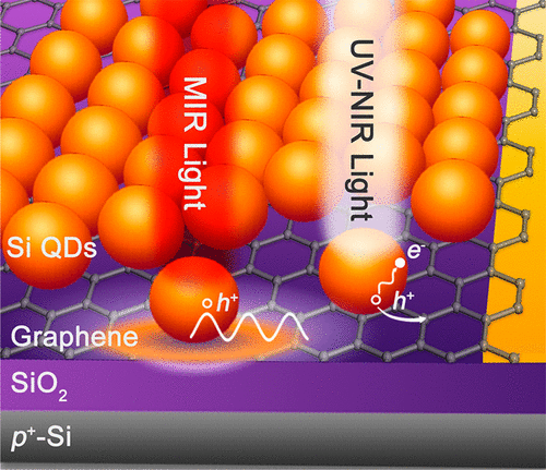
Plasmonic Silicon Quantum Dots Enabled High-Sensitivity Ultrabroadband Photodetection of Graphene-Based Hybrid Phototransistors
ACS Nano ( IF 15.8 ) Pub Date : 2017-09-22 00:00:00 , DOI: 10.1021/acsnano.7b03569 Zhenyi Ni , Lingling Ma , Sichao Du , Yang Xu , Meng Yuan , Hehai Fang 1 , Zhen Wang 1 , Mingsheng Xu , Dongsheng Li , Jianyi Yang , Weida Hu 1 , Xiaodong Pi , Deren Yang
ACS Nano ( IF 15.8 ) Pub Date : 2017-09-22 00:00:00 , DOI: 10.1021/acsnano.7b03569 Zhenyi Ni , Lingling Ma , Sichao Du , Yang Xu , Meng Yuan , Hehai Fang 1 , Zhen Wang 1 , Mingsheng Xu , Dongsheng Li , Jianyi Yang , Weida Hu 1 , Xiaodong Pi , Deren Yang
Affiliation
|
Highly sensitive photodetection even approaching the single-photon level is critical to many important applications. Graphene-based hybrid phototransistors are particularly promising for high-sensitivity photodetection because they have high photoconductive gain due to the high mobility of graphene. Given their remarkable optoelectronic properties and solution-based processing, colloidal quantum dots (QDs) have been preferentially used to fabricate graphene-based hybrid phototransistors. However, the resulting QD/graphene hybrid phototransistors face the challenge of extending the photodetection into the technologically important mid-infrared (MIR) region. Here, we demonstrate the highly sensitive MIR photodetection of QD/graphene hybrid phototransistors by using plasmonic silicon (Si) QDs doped with boron (B). The localized surface plasmon resonance (LSPR) of B-doped Si QDs enhances the MIR absorption of graphene. The electron-transition-based optical absorption of B-doped Si QDs in the ultraviolet (UV) to near-infrared (NIR) region additionally leads to photogating for graphene. The resulting UV-to-MIR ultrabroadband photodetection of our QD/graphene hybrid phototransistors features ultrahigh responsivity (up to ∼109 A/W), gain (up to ∼1012), and specific detectivity (up to ∼1013 Jones).
中文翻译:

等离子体硅量子点实现了基于石墨烯的混合光电晶体管的高灵敏度超宽带光电检测。
甚至接近单光子水平的高灵敏度光电检测对于许多重要应用而言都至关重要。基于石墨烯的混合光电晶体管特别适合用于高灵敏度光电检测,因为它们由于石墨烯的高迁移率而具有很高的光电导增益。鉴于其出色的光电性能和基于溶液的处理,胶体量子点(QD)已被优先用于制造基于石墨烯的混合光电晶体管。但是,最终的QD /石墨烯混合光电晶体管面临着将光电检测扩展到技术上重要的中红外(MIR)区域的挑战。在这里,我们演示了通过使用掺有硼(B)的等离子硅(Si)QD来对QD /石墨烯混合光电晶体管进行高灵敏度的MIR光电探测。B掺杂Si量子点的局部表面等离子体共振(LSPR)增强了石墨烯的MIR吸收。掺杂B的Si QD在紫外(UV)到近红外(NIR)区域的基于电子跃迁的光吸收另外会导致石墨烯的光门化。我们的QD /石墨烯混合光电晶体管产生的UV-MIR超宽带光电检测具有超高的响应度(高达〜109 A / W),增益(高达〜10 12)和比探测率(高达〜10 13 Jones)。
更新日期:2017-09-22
中文翻译:
等离子体硅量子点实现了基于石墨烯的混合光电晶体管的高灵敏度超宽带光电检测。
甚至接近单光子水平的高灵敏度光电检测对于许多重要应用而言都至关重要。基于石墨烯的混合光电晶体管特别适合用于高灵敏度光电检测,因为它们由于石墨烯的高迁移率而具有很高的光电导增益。鉴于其出色的光电性能和基于溶液的处理,胶体量子点(QD)已被优先用于制造基于石墨烯的混合光电晶体管。但是,最终的QD /石墨烯混合光电晶体管面临着将光电检测扩展到技术上重要的中红外(MIR)区域的挑战。在这里,我们演示了通过使用掺有硼(B)的等离子硅(Si)QD来对QD /石墨烯混合光电晶体管进行高灵敏度的MIR光电探测。B掺杂Si量子点的局部表面等离子体共振(LSPR)增强了石墨烯的MIR吸收。掺杂B的Si QD在紫外(UV)到近红外(NIR)区域的基于电子跃迁的光吸收另外会导致石墨烯的光门化。我们的QD /石墨烯混合光电晶体管产生的UV-MIR超宽带光电检测具有超高的响应度(高达〜109 A / W),增益(高达〜10 12)和比探测率(高达〜10 13 Jones)。


 京公网安备 11010802027423号