Our official English website, www.x-mol.net, welcomes your
feedback! (Note: you will need to create a separate account there.)
Direct Vapor Growth of Perovskite CsPbBr3 Nanoplate Electroluminescence Devices
ACS Nano ( IF 15.8 ) Pub Date : 2017-09-22 00:00:00 , DOI: 10.1021/acsnano.7b03660 Xuelu Hu 1 , Hong Zhou 1 , Zhenyu Jiang 1 , Xiao Wang 1 , Shuangping Yuan 1 , Jianyue Lan 2 , Yongping Fu 3 , Xuehong Zhang 1 , Weihao Zheng 1 , Xiaoxia Wang 1 , Xiaoli Zhu 1 , Lei Liao 1 , Gengzhao Xu 2 , Song Jin 3 , Anlian Pan 1
ACS Nano ( IF 15.8 ) Pub Date : 2017-09-22 00:00:00 , DOI: 10.1021/acsnano.7b03660 Xuelu Hu 1 , Hong Zhou 1 , Zhenyu Jiang 1 , Xiao Wang 1 , Shuangping Yuan 1 , Jianyue Lan 2 , Yongping Fu 3 , Xuehong Zhang 1 , Weihao Zheng 1 , Xiaoxia Wang 1 , Xiaoli Zhu 1 , Lei Liao 1 , Gengzhao Xu 2 , Song Jin 3 , Anlian Pan 1
Affiliation
|
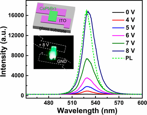
Metal halide perovskite nanostructures hold great promises as nanoscale light sources for integrated photonics due to their excellent optoelectronic properties. However, it remains a great challenge to fabricate halide perovskite nanodevices using traditional lithographic methods because the halide perovskites can be dissolved in polar solvents that are required in the traditional device fabrication process. Herein, we report single CsPbBr3 nanoplate electroluminescence (EL) devices fabricated by directly growing CsPbBr3 nanoplates on prepatterned indium tin oxide (ITO) electrodes via a vapor-phase deposition. Bright EL occurs in the region near the negatively biased contact, with a turn-on voltage of ∼3 V, a narrow full width at half-maximum of 22 nm, and an external quantum efficiency of ∼0.2%. Moreover, through scanning photocurrent microscopy and surface electrostatic potential measurements, we found that the formation of ITO/p-type CsPbBr3 Schottky barriers with highly efficient carrier injection is essential in realizing the EL. The formation of the ITO/p-type CsPbBr3 Schottky diode is also confirmed by the corresponding transistor characteristics. The achievement of EL nanodevices enabled by directly grown perovskite nanostructures could find applications in on-chip integrated photonics circuits and systems.
中文翻译:

钙钛矿CsPbBr 3纳米板电致发光器件的直接气相生长
金属卤化物钙钛矿纳米结构因其优异的光电性能而有望作为集成光子的纳米级光源。然而,使用卤化钙钛矿可以溶解在传统器件制造工艺中所需的极性溶剂中,使用传统的光刻方法来制造卤化钙钛矿纳米器件仍然是一个巨大的挑战。在本文中,我们报道了单CsPbBr 3纳米板电致发光(EL)器件制造通过直接生长CsPbBr 3电极上氧化预图案化铟锡纳米片(ITO)通过气相沉积。明亮的EL出现在负偏压触点附近的区域中,其开启电压约为3 V,半峰全宽为22 nm,全宽较窄,外部量子效率约为0.2%。此外,通过扫描光电流显微镜和表面静电势测量,我们发现利用高效载流子注入形成ITO / p型CsPbBr 3肖特基势垒对于实现EL至关重要。ITO / p型CsPbBr 3肖特基二极管的形成还可以通过相应的晶体管特性来确认。通过直接生长钙钛矿纳米结构实现的EL纳米器件的成就可以在片上集成光子电路和系统中找到应用。
更新日期:2017-09-22
中文翻译:
钙钛矿CsPbBr 3纳米板电致发光器件的直接气相生长
金属卤化物钙钛矿纳米结构因其优异的光电性能而有望作为集成光子的纳米级光源。然而,使用卤化钙钛矿可以溶解在传统器件制造工艺中所需的极性溶剂中,使用传统的光刻方法来制造卤化钙钛矿纳米器件仍然是一个巨大的挑战。在本文中,我们报道了单CsPbBr 3纳米板电致发光(EL)器件制造通过直接生长CsPbBr 3电极上氧化预图案化铟锡纳米片(ITO)通过气相沉积。明亮的EL出现在负偏压触点附近的区域中,其开启电压约为3 V,半峰全宽为22 nm,全宽较窄,外部量子效率约为0.2%。此外,通过扫描光电流显微镜和表面静电势测量,我们发现利用高效载流子注入形成ITO / p型CsPbBr 3肖特基势垒对于实现EL至关重要。ITO / p型CsPbBr 3肖特基二极管的形成还可以通过相应的晶体管特性来确认。通过直接生长钙钛矿纳米结构实现的EL纳米器件的成就可以在片上集成光子电路和系统中找到应用。


 京公网安备 11010802027423号