Our official English website, www.x-mol.net, welcomes your
feedback! (Note: you will need to create a separate account there.)
Catching the electron in action in real space inside a Ge–Si core–shell nanowire transistor
Nanoscale ( IF 5.8 ) Pub Date : 2017-09-01 00:00:00 , DOI: 10.1039/c7nr05589g Meghnath Jaishi 1, 2, 3, 4 , Ranjit Pati 1, 2, 3, 4, 5
Nanoscale ( IF 5.8 ) Pub Date : 2017-09-01 00:00:00 , DOI: 10.1039/c7nr05589g Meghnath Jaishi 1, 2, 3, 4 , Ranjit Pati 1, 2, 3, 4, 5
Affiliation
|
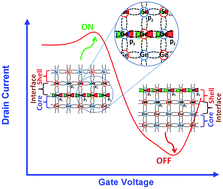
Catching the electron in action in real space inside a semiconductor Ge–Si core–shell nanowire field effect transistor (FET), which has been demonstrated (J. Xiang, W. Lu, Y. Hu, Y. Wu, H. Yan and C. M. Lieber, Nature, 2006, 441, 489) to outperform the state-of-the-art metal oxide semiconductor FET, is central to gaining unfathomable access into the origin of its functionality. Here, using a quantum transport approach that does not make any assumptions on electronic structure, charge, and potential profile of the device, we unravel the most probable tunneling pathway for electrons in a Ge–Si core–shell nanowire FET with orbital level spatial resolution, which demonstrates gate bias induced decoupling of electron transport between the core and the shell region. Our calculation yields excellent transistor characteristics as noticed in the experiment. Upon increasing the gate bias beyond a threshold value, we observe a rapid drop in drain current resulting in a gate bias driven negative differential resistance behavior and switching in the sign of trans-conductance. We attribute this anomalous behavior in drain current to the gate bias induced modification of the carrier transport pathway from the Ge core to the Si shell region of the nanowire channel. A new experiment involving a four probe junction is proposed to confirm our prediction on gate bias induced decoupling.
中文翻译:

在Ge-Si核-壳纳米线晶体管内部的现实空间中捕获电子
在半导体Ge-Si核-壳纳米线场效应晶体管(FET)内的实际空间中捕获电子的行为已得到证明(J. Xiang,W. Lu,Y. Hu,Y. Wu,H. Yan和CM Lieber,《自然》,2006年,第441页(第489页),其性能优于最先进的金属氧化物半导体FET,对于获得对其功能起源的深入了解至关重要。在这里,使用一种不对器件的电子结构,电荷和电势分布进行任何假设的量子传输方法,我们在具有轨道水平空间分辨率的Ge-Si核-壳纳米线FET中揭示了电子最可能的隧穿路径,这证明了栅极偏置引起的核与壳区域之间电子传输的解耦。我们的计算得出了实验中注意到的出色的晶体管特性。将栅极偏置增加到超过阈值后,我们观察到漏极电流迅速下降,从而导致栅极偏置驱动负差分电阻行为并切换跨导符号。我们将这种在漏极电流中的异常行为归因于栅极偏置引起的载流子从Ge核到纳米线沟道的Si壳区域的载流子传输路径的修饰。提出了一个涉及四个探针结的新实验,以确认我们对栅极偏置引起的去耦的预测。
更新日期:2017-09-21
中文翻译:
在Ge-Si核-壳纳米线晶体管内部的现实空间中捕获电子
在半导体Ge-Si核-壳纳米线场效应晶体管(FET)内的实际空间中捕获电子的行为已得到证明(J. Xiang,W. Lu,Y. Hu,Y. Wu,H. Yan和CM Lieber,《自然》,2006年,第441页(第489页),其性能优于最先进的金属氧化物半导体FET,对于获得对其功能起源的深入了解至关重要。在这里,使用一种不对器件的电子结构,电荷和电势分布进行任何假设的量子传输方法,我们在具有轨道水平空间分辨率的Ge-Si核-壳纳米线FET中揭示了电子最可能的隧穿路径,这证明了栅极偏置引起的核与壳区域之间电子传输的解耦。我们的计算得出了实验中注意到的出色的晶体管特性。将栅极偏置增加到超过阈值后,我们观察到漏极电流迅速下降,从而导致栅极偏置驱动负差分电阻行为并切换跨导符号。我们将这种在漏极电流中的异常行为归因于栅极偏置引起的载流子从Ge核到纳米线沟道的Si壳区域的载流子传输路径的修饰。提出了一个涉及四个探针结的新实验,以确认我们对栅极偏置引起的去耦的预测。


 京公网安备 11010802027423号